A simple application, ARM chip as master, flash as slaver, realize one-to-one communication. ARM main control chip STM32F103, flash chip is MX25L6465E of MACRONIX INTERNATIONAL, 64Mbit. SPI should be the simplest kind of application in embedded peripherals! Generally, there are two methods for SPI application: software simulation, manual simulation to generate timing and application of the SPI controller of the main control chip. Generally, the second method is better and more stable. The main points of applying the SPI controller of the main control chip are: correctly initialize the SPI, operate the SPI registers, and correctly understand the timing of the flash. The following is the process, using the library function that comes with STM32F10X 1. Initialization: void SpiFlashIniTIalzaTIon(void); To know how the hardware is connected, whether SPI1 or SPI2 is connected to the flash, through the connection diagram we know that we are going to operate SPI2. Initialization is about 3 parts, configure the clock; configure GPIO; configure SPI2. It should be noted here that the CS chip selection pin is used as an ordinary GPIO, the output mode is "push-pull output", and the other CLK, MISO, MOSI are "multi-function push-pull output"; Code: void SpiFlashIniTIalzaTIon(void) { /*Initialized SPI, GPIO structure*/ SPI_InitTypeDef SPI_InitStructure; GPIO_InitTypeDef GPIO_InitStructure; RCC_APB1PeriphClockCmd( RCC_APB1Periph_SPI2, ENABLE); /*Enable SPI2 clock (bit 14) in RCC_APB1ENB*/ RCC_APB2PeriphClockCmd( RCC_APB2Periph_GPIOB, ENABLE);/*Because the 4 pins related to SPI2 and GPIOB phase*/ /*Off, GPIOB clock (bit 3), this sentence is not yet*/ /*Determine whether it is necessary or not, and then confirm when debugging*/ /*The above sentence is necessary, because the CS pin is used as a GPIO, 2011-01-30 debugging*/ /*Configure SPI_FLASH_CLK(PB13), SPI_FLASH_MISO(PB14), SPI_FLASH_MOSI(PB15)*/ GPIO_InitStructure.GPIO_Pin=GPIO_Pin_13 | GPIO_Pin_14 | GPIO_Pin_15; GPIO_InitStructure.GPIO_Mode=GPIO_Mode_AF_PP; /*Multiple function push-pull output*/ GPIO_InitStructure.GPIO_Speed=GPIO_Speed_50MHz; GPIO_Init( GPIOB, &GPIO_InitStructure); /*Configuration input SPI_FLASH_CS(PB12)*/ GPIO_InitStructure.GPIO_Pin=GPIO_Pin_12; GPIO_InitStructure.GPIO_Mode=GPIO_Mode_Out_PP; /*Push-pull output*/ GPIO_InitStructure.GPIO_Speed=GPIO_Speed_50MHz; GPIO_Init( GPIOB, &GPIO_InitStructure); SPI_FLASH_CS_SET; /*Do not select flash*/ /* SPI2 configuration added in 2010-01-13*/ /* Note: In SPI_NSS_Soft mode, the SSI bit determines the level of (PB12) on the NSS pin. * When SSM=1, the NSS pin is released, and the NSS pin can be used as a GPIO port*/ SPI_InitStructure.SPI_Direction = SPI_Direction_2Lines_FullDuplex; /*Bidirectional bidirectional full duplex BIDI MODE=0*/ SPI_InitStructure.SPI_Mode = SPI_Mode_Master; /*SSI bit is 1, MSTR bit is 1*/ SPI_InitStructure.SPI_DataSize = SPI_DataSize_8b; /*SPI sending and receiving 8-bit frame structure*/ SPI_InitStructure.SPI_CPOL = SPI_CPOL_High; /*CPOL=1,CPHA=1, mode 3*/ SPI_InitStructure.SPI_CPHA = SPI_CPHA_2Edge; SPI_InitStructure.SPI_NSS = SPI_NSS_Soft; /*The internal NSS signal is controlled by the SSI bit, SSM=1*/ SPI_InitStructure.SPI_BaudRatePrescaler = SPI_BaudRatePrescaler_4; /*Baud rate prescaler value is 4*/ SPI_InitStructure.SPI_FirstBit = SPI_FirstBit_MSB; /*Data transmission starts from MSB*/ SPI_InitStructure.SPI_CRCPolynomial = 7; /*Reset default value*/ SPI_Init(SPI_SELECT, &SPI_InitStructure); SPI_Cmd(SPI_SELECT,ENABLE); /*Enable SPI2*/ } 2. Operate the SPI controller correctly; What needs attention here is to understand the SPI status register, especially SPI_SR bit 7 busy flag bit BSY to be careful, each time you operate SPI, you must first read SPI_SR, BSY is not busy before the next step, and then the buffer is operated. There is another problem that has troubled me for a long time. The timing problem of SPI is how CLK outputs timing. Finally, my understanding is that every time SPI sends a byte, CLK will automatically generate timing. If it is not sent, CLK will stop. This saves power consumption. Therefore, if SPI wants to receive a byte, it must first send a byte, for example, send a SPI_DUMMY_BYTE, some of the dummy byte flash has definitions and some do not, if not, define one by yourself, as long as it is not the same as the command word. u8 SpiFlashSendByte(u8 send_data); u8 SpiFlashReceiveByte(void); Code: /*Function: SPI sends a byte *Parameter: send_data: bytes to be sent *Return: None*/ u8 SpiFlashSendByte(u8 send_data) { /*Check the Busy bit, bit 7 in the SR of SPI, whether the SPI communication is busy, until it is not busy to jump out*/ //while( SET==SPI_I2S_GetFlagStatus(SPI_SELECT, SPI_I2S_FLAG_BSY)); /*Check the TXE bit, bit 1 in the SR of SPI, whether the transmit buffer is empty, until the empty jumps out*/ while( RESET==SPI_I2S_GetFlagStatus(SPI_SELECT,SPI_I2S_FLAG_TXE)); SPI_I2S_SendData(SPI_SELECT, send_data); /*Send one byte*/ /*Receive one byte after sending data*/ while( RESET==SPI_I2S_GetFlagStatus(SPI_SELECT, SPI_I2S_FLAG_RXNE) ); return( SPI_I2S_ReceiveData(SPI_SELECT) ); } /*Function: SPI receives a byte of flash *Parameter: received byte *Return: None*/ u8 SpiFlashReceiveByte(void) { /*Check the RXNE bit, bit 0 in the SR of SPI, to make sure that the receive buffer has data*/ return(SpiFlashSendByte(SPI_DUMMY_BYTE)); } 3. Understand the read and write operations of flash First of all, it must be erased before data is written, because all flashes can only be changed from 1 to 0. Erasing sets all flashes to 1, and the corresponding bit is 0 when writing. In this part of the read and write operation, the flash chip manual describes the operation steps in detail. What needs to be noted is the status register of the flash MX25L64. Before operating the flash, first read flash_SR, make sure WIP=0 (flash is idle), and make sure WEL=1 for operations such as flash erasing and programming (flash can accept operations such as erasing and programming). When writing to flash, it is necessary to understand one point: writing data to flash (that is, Page Program (PP), Command 02) is based on the page (256bytes) unit, if the data is written to the end of the page, it will start from the current page Continue to write the remaining data at the first address, which may cause the loss of data, just pay attention! Mainly to understand this paragraph in the manual: The Page Program(PP) instruction is for programming the memory to be "0"......If the eight least significant address bits(A7-A0) are not all 0, all transmitted data going beyond the end of the current page are grogrammed from the start address of the same page(from the address A7-A0 are all 0).If more than 256 bytes are sent to the device,the data of the last 256 -byte is programmed at the requtest page and previous data will be disregarded. If less than 256 bytes ....... Code: /*Function: Start reading data from flash at the specified address Parameter: pData_from_flash, the pointer to store the read data address_to_read, the starting address of the data to be read, the valid bits of the address format are: A23-A0 Return: Pointer to the read data pData_from_flash */ void SpiFlashReadData( u8 *pData_from_flash, u Electronic Components Resistor
Resistor (Resistor) commonly known as resistance directly in our daily life.It is a current limiting element. When the resistance is connected to the circuit, the resistance value of the resistor is fixed, usually two pins.Fixed resistors are those whose resistances cannot be changed.Resistance variable is called potentiometer or variable resistor.The ideal resistor is linear, that is, the instantaneous current through the resistor is proportional to the applied instantaneous voltage.Variable resistor for partial pressure.On the exposed resistor body, one or two movable metal contacts are pressed tightly.The contact position determines the resistance between any end of the resistance body and the contact.
Flat tube resistor
Electronic Components Resistor,Metal Film Resistor,Metal Oxide Film Resistor YANGZHOU POSITIONING TECH CO., LTD. , https://www.pst-thyristor.com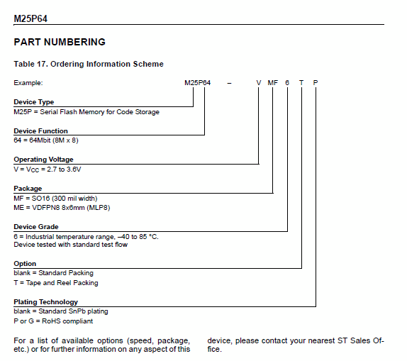
Metal aluminum shell resistor
Stainless steel resistor box
Crowbar (wind power converter) resistor
RX21 Glazed Wirewound Resistor
RX21 Glazed Power Wirewound Resistor
Inverter ceramic resistor
Resistor Cabinet
Resistive load box
Ultra-thin aluminum shell resistor
High power resistor
water cooling resistor
RI80 high voltage resistor
RX20 High Power Painted Wirewound Resistor
stainless steel resistor
Howo resistor
KNP Porcelain Rod Painted Wirewound Resistor
Cement Resistor
Thick Film Resistors
