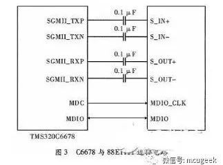
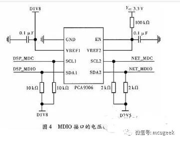
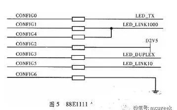
For the data communication between the 8-core DSP TMS320C6678 and external devices, the integrated chip Gigabit Ethernet switching subsystem is taken as the core, and the chip 88E1111 is selected as the PHY device, and the hardware circuit of the Gigabit Ethernet communication interface is designed. In the embedded operating system SYS/BIOS and network development environment NDK, the programming of the underlying Ethernet driver and TCP/IP protocol is completed. The Ethernet communication test with the host computer through the DSP proves the correctness and practicability of the hardware and software of the Ethernet interface circuit. As DSP processors become more widely used in modern industries, DSP functions not only require fast arithmetic processing, but also real-time data exchange with other processors or devices to achieve resource sharing. Therefore, for a variety of equipment needs, the choice of a stable, fast and efficient interface is a key component in today's digital signal processing system design. TI's 8-core processor TMS320C6678 (hereafter referred to as C6678) provides a wealth of on-chip interface resources for communication between the processor and peripherals. These interfaces can be used for communication between DSP and peripherals, but flexibility Differences, using the SGMII interface to achieve Gigabit Ethernet communication, can make the communication interface general, can be applied to a large number of device connections. This paper designs and implements Gigabit Ethernet communication for the chip characteristics of C6678 and the interface resources. It mainly designs the Ethernet interface circuit, the network underlying hardware driver, the TCP/IP protocol user program, and completes the Ethernet with the host computer. Communication test realizes high-speed and efficient network transmission of digital signals. The C6678 is an 8-core high-performance, fixed-point/floating point processor based on the KeyStone I architecture with a single core operating at up to 1.25 GHz. The Ethernet switching subsystem of the C6678 includes two Ethernet Media Access Controllers (EMACs), two SGMIIs, one Management Data Input Output (MDIO), and a 3-Port Ethernet Switching Module. And the network configuration bus, its network switching subsystem is shown in Figure 1. The function of EMAC is to convert the internal signal of the switching subsystem into GMII signal to the SGMII module; the MDIO control physical layer chip performs control input and output on the multi-data stream. This paper chooses C6678 as the main chip. Since the G6 network switching subsystem of C6678 only supports SGMII interface, this paper selects the physical chip 88E1111 which has better compatibility with the network data transmission of SGMII interface. The internal structure of 88E1111 chip is shown in Figure 2. Show. The media interface of the 88E1111 has a copper media interface and a fiber interface. The copper media interface is MDI[3:0], and the operating mode is selected by setting HWCFG_MODE[3:0]. The 88E1111 integrated MDIO module is connected to the MDIO interface of the EMAC, which can facilitate the network control terminal to read the physical chip status register to achieve real-time monitoring. The task of this paper is based on the interface design of the C6678 on-chip Ethernet switching subsystem and the off-chip PHY chip 88E1111 and its peripheral circuits. Mainly include: C6678 and 88E1111 chip connection, 88E1111 chip configuration and 88E1111 chip and network media connection. 3.1 C6678 and 88E1111 chip connection The interface circuit of C6678 and PHY chip 88E1111 is shown as in Fig. 3. The 88E1111 operates in the SGMII interface mode and does not require the TXCLK clock input. It helps reduce the number of traces on the board and also reduces noise. The main interface signals include clock and data signals as follows: MDIO_CLK: Manages the data clock. This clock signal is provided by the MD6 module on the C6678 chip, which is controlled by configuring the CLKDIV bit in the MDIO control register, CONTROL. SGMII_TXP and SGMII_TXN: Serial transmit differential data lines. Connect the internal SerDes of the DSP and the S_IN pin of the physical chip. The SerDes of the DSP sends serial data to the physical layer through the pin, and the data includes the transmit data clock signal. SGMII_RXP and SGMII_RXN: Serial receive differential data lines. Connect the internal SerDes of the DSP and the S_OUT pin of the physical chip. The physical layer chip transmits data to the SerDes of the DSP through the interface, and the data includes the data receiving clock signal. MDIO: Manage data I/O. Up to 32 PHY devices can be connected to the EMAC of the DSP, and all PHY devices can be enumerated, and the PHY device status register can be read to monitor the connection status of the PHY. The data frame structure conforms to the 802.3 standard and includes read and write instructions, PHY addresses, register addresses, and data. Because the integrated MDIO on the 88E1111 is connected to the C6678 integrated MDIO module, the voltage is different. The former voltage is 2.5 V and the latter voltage is 1.8 V. Therefore, a voltage converter should be added between the two. This article uses a PCA9306 to achieve level shifting between 2.5 V and 1.8 V. The connection circuit is shown in Figure 4. 3.2 88E1111 chip configuration The 88E1111 is connected to the MDIO module of the C6678. The MDIO can identify up to 32 physical chips. It needs to be configured before using the physical chip. The configuration content mainly includes the address and mode of the chip. Configure the CONFTG[6:0] pin definition to query the literature. The hardware circuit configured in this paper is shown in Figure 5. In Figure 5, the resistor can be omitted. For the convenience of testing, add a 0 Ω resistor. After the hardware configuration of 88E1111 is completed, the system will be fixed as an interface mode. According to the definition of the document, the address of the physical chip is: PHY_ADDRESS=0'b00001, and the chip mode is: SGMII mode without auto-negotiation with clock. 3.3 88E1111 chip and RJ45 connection The 88E1111 and the network medium cannot be directly connected. Because the transmission speed is in the gigabit class, it is more necessary to design a suitable network isolation transformer to reduce transmission loss, echo and crosstalk. This article selects the Gigabit Ethernet port socket HR911130C, which has its own transformer circuit. It only needs to connect the filter network externally to realize the stable transmission of the network signal. The 88E1111 and HR9111130C use differential connections, which require strict equal lengths in PCB layout, and generally require an impedance matching network, such as R1 and C1 in Figure 6. TI has released a Network Development Kit (NDK) for network development, which can transfer the configuration operations of multiple modules to the NDK network framework. At the same time, data subcontracting and parsing do not require too much consideration by programmers, which accelerates network development. process. The NDK is built on top of the real-time operating system SYS/BIOS. The NDK interacts with the BIOS through the OS abstraction layer. The BIOS cfg configuration file can visually view the NDK modules. Auto Radiator,Car Radiator,Car Coolant,Car Engine Coolant Huangshan Kaichi Technology Co.,Ltd , https://www.kaichitech.com
C6678 chip features and interface resources
DSP application