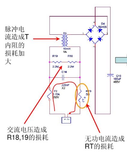
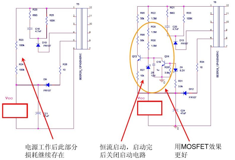
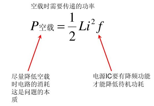
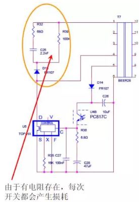
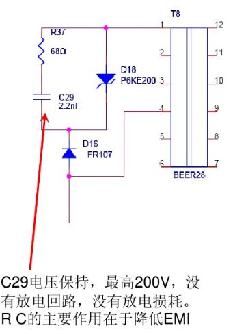
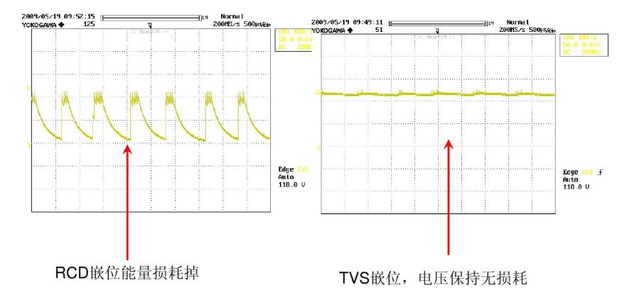
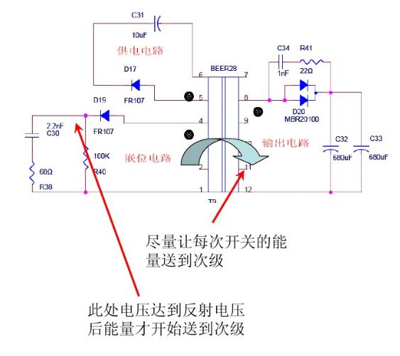
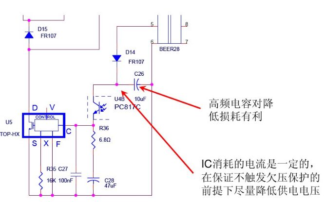
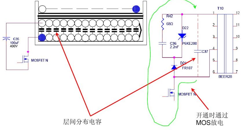
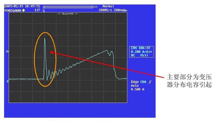
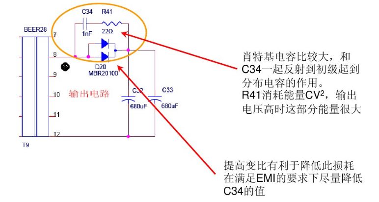
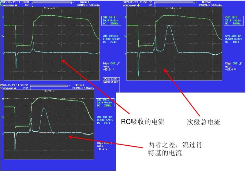
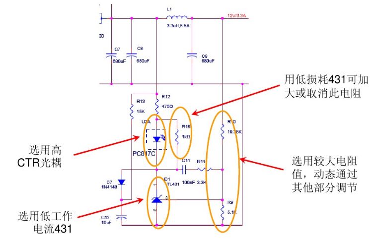
. The "standby power" problem of the switching power supply should be solved like this! ! ! Input partial loss 1. The internal resistance loss of the common mode inductor T caused by the pulse current is increased. Properly design common mode inductors, including wire diameter and turns 2. Loss on the discharge resistor Increase the organization of the discharge resistor under the premise of compliance with safety regulations 3. Loss on the thermistor Reduce the resistance of the thermistor while meeting other indicators Start loss Ordinary starting method, the starting resistor circuit is not cut off after the switching power supply is started, and the loss persists. Improvement method: The constant current startup mode is started, and the startup circuit is turned off after the startup is completed to reduce the loss. Loss associated with switching power supply operation Clamp circuit loss There is a discharge resistor, and the mos switch will generate discharge loss every time it is switched. Improvement method: Using TVS clamp as shown below, the resistance discharge loss can be eliminated (Note: The resistance discharge loss can only be reduced here, and the peak loss caused by leakage inductance energy cannot be avoided) Of course, the most fundamental improvement is to reduce the leakage inductance of the transformer. Power supply winding loss The power chip needs a certain current and voltage to work. If the Vcc supply voltage is higher, the loss will be larger. Improvement method: Since the current consumed by the IC is constant, the Vcc supply voltage can be reduced as much as possible while ensuring that the chip can be in the safe working voltage range! Transformer loss Since the effective operating frequency is low during standby, and the current current limit is small, the flux change is small, the core loss is small, and the standby has little effect, but the winding loss is not negligible. Loss caused by transformer windings The charge-discharge loss of the distributed capacitance between the layers of the winding (the distributed capacitance is charged when the switching MOS transistor is turned off, and the loss caused by the discharge when the switching MOS transistor is turned on.) When testing the mos tube current waveform, there is a current spike that is mainly caused by the transformer distributed capacitance when it is turned on. Improvement method: Insulate tape between the winding layer and the layer to reduce the distribution capacitance between the layers. Loss on the switching transistor MOSFET Mos losses include: conduction loss, switching loss, and drive loss. The biggest loss in the standby state is the switching loss. Improvement method: reduce the switching frequency, use inverter chip or even frequency hopping chip (the chip enters intermittent oscillation under no-load or very light load) Absorption loss on the rectifier The junction capacitance on the output rectifier and the snubber current of the rectifier in the switching state are reflected to the primary loop, causing switching losses. There is also a loss due to charge and discharge of the resistor on the snubber circuit. Improvement method: Under the premise of other indicators, try to reduce the capacitance of the absorption capacitor and reduce the resistance of the absorption resistor. Of course, there are switching losses, conduction losses, and reverse recovery losses on the rectifier. This should, if possible, choose diodes with reduced turn-on voltage and short reverse recovery times. Output feedback circuit loss Outdoor Fiber Cable,Outdoor Fiber,2 Core Outdoor Fiber Optic Cable,2 Core Outdoor Cable Zhejiang Wanma Tianyi Communication Wire & Cable Co., Ltd. , https://www.zjwmty.com