-
Model NO.: pcb-459
-
Dielectric: FR-4
-
Application: Aerospace
-
Mechanical Rigid: Rigid
-
Base Material: Copper
-
Brand: JC
-
Land Area of Our Factory: More Than 10000 Square Meter
-
PCB Layers: 1~16
-
PCB Max. Size: 1200mm×600mm
-
Certificate: RoHS, ISO14000, SGS, UL,Reach
-
Specification: TS16949, SGS, ISO14000, REACH, RoHS
-
Type: Rigid Circuit Board
-
Material: Fiberglass Epoxy
-
Flame Retardant Properties: V0
-
Processing Technology: Electrolytic Foil
-
Insulation Materials: Epoxy Resin
-
We Found: in 1998
-
Business Nature: Manufacturing of Printed Circuit Board
-
PCB Surface Finishes: HASL(Lead Free), Enig, OSP, Gold Finger, Tin, etc.
-
Laminate Materials: Fr-4,Fr-1,,Fr-2,Cem-1,Cem-3
-
Trademark: HRSC
-
Origin: Dongguan
                                                          HRSC PCB Manufacturer
We are the Printed Circuit Boards (PCB) manufacturer with 15 years experience, specialized in single-sided, 2-layerd, multilayer and high density interconnector (HDI) PCB. We take strict Japanese-pattern management, so please trust us with your orders!
Our PCBs are used for auto industry, high power led, Office Appliance, electric toy, machinery, industrial lighting and so on.
Our Corporate Vision: To become the world's most trustful PCB
Our Corporate Values: Excellence, customer satisfaction, innovation and integrity, green.
Our Quality Target:
1.Ptoduction pass rate>99%
2.Timely delivery rate>98%
3.Customer complaint rate<1%
4.Customer satisfaction rate>99%
Environmental Guideline:
Protect the environment, prevent pollution, save resources, and reduce waste.
PCB Manufacture Quality Control:
1. Engineering pretreatment before production
2. 100% E-test, 100% visual inspection
3. AOI inspection
4. High voltage test, impedance control test
5. Micro section, soldering capacity, thermal, shocking test
6. Reliability test, insulating resistance test, ionic cleanliness testing
Our PCB process capability
PCB Description |
Our PCB Board Capability |
| PCB Surface Finishes |
electrolytic nickel-gold,
HASL(Lead Free, ENIG (Electroless Nickel/Immersion Gold, Carbon Ink, Golden Fingers, OSP (Entek, Immersion Tin, Immersion Silver |
| PCB Max. Size |
1200mm×600mm |
| PCB Min. Size |
5mm×5 mm |
| Bow & Twist Tolerance |
Single Side≤1.0%,Double Side≤0.7%, Muti-Layer≤0.5% |
| Min. Board Thickness & Tolerance |
0.2mm±0.08mm |
| PCB Min. trace/spacing |
Tin board:0.2mm±20%(8mil±0%) |
| gold board:0.075mm±20%(3mil±0%) |
| Copper to Board Edge Spacing |
0.5mm(20mil) |
| Hole to Trace Spacing |
0.3mm(12mil) |
| Min. Hole Diameter |
0.2mm±.076mm(8mil±3mil) |
| Min. Hole Clearance |
0.4mm±.076mm(16mil±3mil) |
| Copper Thickness on Hole Wall |
20-25um(0.79mil-1.0mil) |
| Hole Location Tolerance |
±0.076mm(l±3mil) |
| Min Diameter of Punching Hole |
FR-4 board thickness≤1.0mm(40mil):1.0mm(40mil) |
| FR-4 board thickness 1.2-3.0mm(48-120mil):1.5mm(60mil) |
| PCB Min. Punching Slot |
FR-4 CEM-3 board thickness≤1. 0mm(40mil):0.8 mm×0.8 mm(32mil×32mil) |
| FR-4 board thickness1.2-3.0mm(48-120mil): 1.0 mm×1.0 mm(40mil×40mil) |
| Trace width variation |
±0.076mm(±3mil) |
| Outline Tolerance |
Routing:±0.1mm (±4mil) ,Punching:±0.05mm (±2mil) |
| V-CUT Registration Tolerance±0.2mm (±8mil) |
| PCB BOARD Type |
Single-sided, double-sided, multi-layer |
| Major Material |
FR-4, CEM-1,CEM-3, high frequency laminates, Aluminum, NiFe-based, copper base |
| PCB BOARD Thickness |
0.2-3.5mm |
| Base Copper Thickness |
11um 35um 70um 105um |
| Max. aspect ratio(board thickness: hole size) |
8:1 |
| V-Cut Angle Tolerance |
±5° |
| V-Cut Board Thickness |
0.4mm -3.2mm(16mil -128mil) |
| Min SMT Pitch |
0.3mm(12mil) |
| Min. Component mark |
0.15mm(6mil) |
| Min. width of annular ring(finished) |
0.15mm(6mil)/side |
| Min pad opening |
0.076mm(3mil) |
| Min S/M Bridge |
±0.076mm(±3mil) |
| carbon ink board manufacturing capability:1.Impedance Control:20K±10% 2.Hardness:6H 3.bearable friction times :above 200000 times |
What we need:
Please tell us the information as below:
NO. |
Items |
NO. |
Items |
| 1 |
Board for what product |
8 |
Surface Finish |
| 2 |
Number of Layers |
9 |
Board Material |
| 3 |
Copper Thickness(um) |
10 |
Board Thickness(um) |
| 4 |
Solder Mask Color |
11 |
PCB Dimensions(mm) |
| 5 |
Silk Screen Color |
12 |
Min Finished Hole Size(mm) |
| 6 |
Milling |
13 |
Min Clearance(mm) |
| 7 |
Min Track Width(mm) |
14 |
Other special requirements |
PCB Fast delivery:
| Packaging |
Vacuum Packing with desiccant,
Professional Export Carton. |
Delivery
time |
 |
Prototype |
  Mass production
(above 30m) |
| 2L |
Quick turn:24h
Usual time:3-4days |
5-10days |
| 4L |
Quick turn:48 hours;
Usual time:5-6days |
10-15days |
| 6L |
Quick turn:72 hours;
Usual time:6-8days |
10-20days |
| 8L |
Quick turn:72 hours;
Usual time:8-10days |
15-22days |
| 10L |
Quick turn:96 hours;
Usual time:12-14days |
18-25days |
| `` |
`` |
`` |
Please send us your Gerber Files and PCB specifications; we will quote for you within 12 hours.
We always try our best! So we do, we conquer, and we get there!
Contact us!!
PCBA--PCB-PCBA-PCB-PCBA--PCB-PCBA-PCB-PCBA--PCB-PCBA-PCB-PCBA-PCB-PCBA--PCB-PCBA
Product Description:
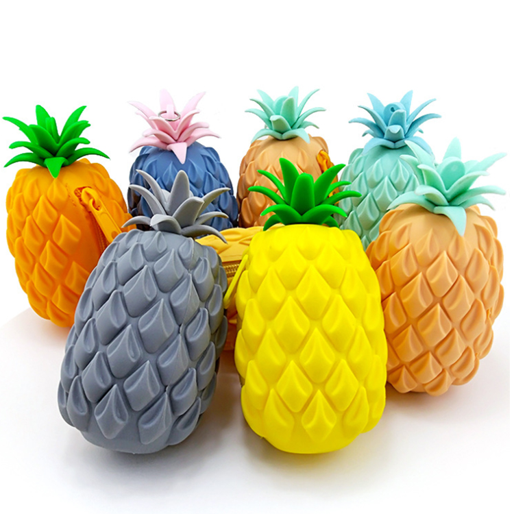
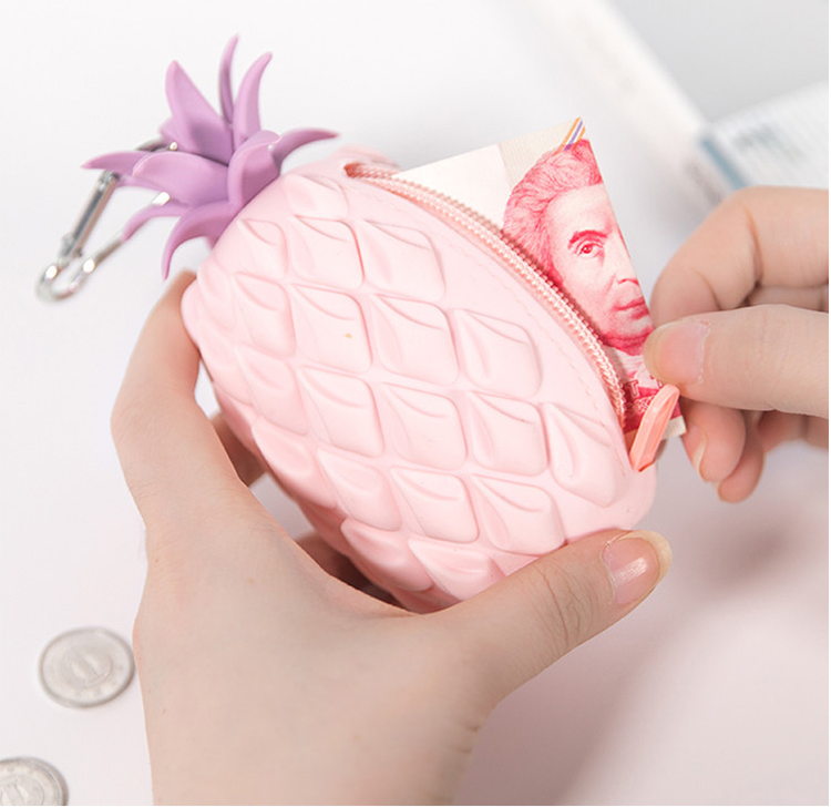
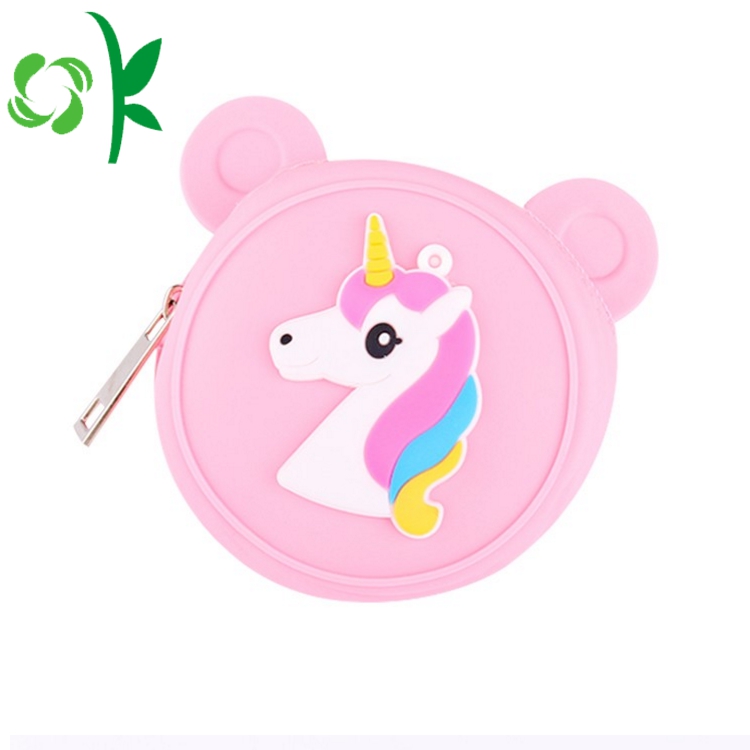
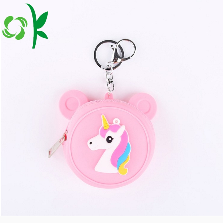
Hey,Do you know Silicone Purse ?We often see leather bags in our daily
life.There are some Silicone Coin Bag wanna introduce you,it's shape
like purse.And it's made of silicone.And Silicone Coin Wallet have many
kinds of size,we call it collectively as XS,S,M,L.And it has many kinds
of purse like Silicone Rubber Purse,Silicone Purses Wholesale,Silicone Jelly Coin Purse, Silicone Coin Purse .
And silicone is kinds of
enviromental material,and it will be cheaper than leather bags,and is
good for enviromental protection.It has many design,and suitable for all
people,especially for women/girls.
Product introduction:
1.Product name:Silicone Coin Bag,Silicone Coin Wallet,Silicone Rubber Purse,Silicone Purses Wholesale,Silicone Jelly Coin Purse,Silicone Coin Purse
2.Place of origin:Guangdong China
3.Color:any pantone color
4.Logo:Printing,debossed,embossed
5.MOQ:500pcs.
6.Package:1 pcs/opp,customized design is available.
7.Design:Customized/stock
8.Certification:FDA,LFGB,SGS,ROHS,etc.
9.Usage:Use in kitchen baking
10.Silicone purse for women photos for reference.


Silicone Purse
Silicone Coin Bag,Silicone Coin Wallet,Silicone Rubber Purse,Silicone Purses Wholesale,Silicone Jelly Coin Purse,Silicone Coin Purse
OK Silicone Gift Co., Ltd. , http://www.oemsiliconegift.com
