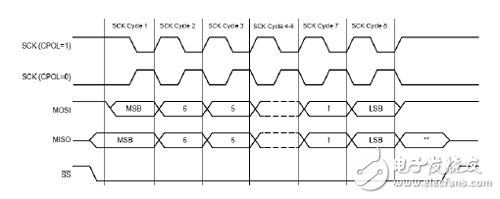
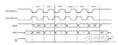
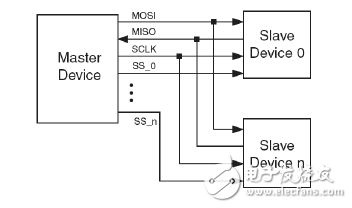
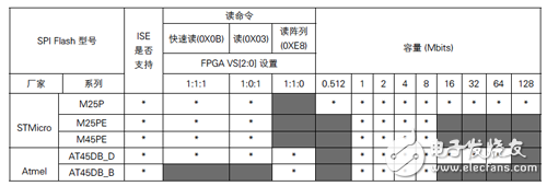
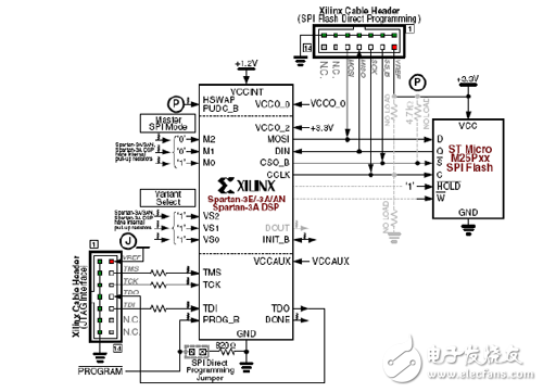
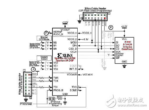
The characteristic of serial flash is that it occupies less pins and is very suitable for data storage of the system. Generally, serial peripheral interface (SPI bus interface) is adopted. The fundamental difference between Flash memory and EEPROM is that EEPROM can rewrite data in bytes, while Flash can only erase an interval and then rewrite its contents. In general, this erasure interval is called a sector, and some manufacturers have introduced the concept of a page. The minimum erase interval is an important indicator when selecting a Flash product. When writing to Flash, if the data written cannot be exactly the size of a minimum erasure interval, it is necessary to save all the data of the entire interval to another storage space, erase the space, and then rewrite the interval. Most Flash processes make it easier to implement larger erase intervals, so Flash in smaller erase intervals is generally slightly more expensive. In addition, SPI is a standard 4-wire synchronous serial bi-directional bus that provides a serial communication data link between the controller and peripherals and is widely used in embedded devices. Xilinx's new FPGAs support the SPI interface. The SPI bus completes the communication between the master and the slave through four signal lines. A typical SPI system often includes a master device and at least one slave device. In the FPGA application, the FPGA chip is the master device, and the SPI serial FLASH is the slave device. equipment. The names and functions of the four SPI interface signals are shown in Table 5-2. Table 5-2 SPI interface signal list A communication interface between a master chip and a slave chip is shown in Figure 5-24. The FPGA controls the timing of the two-side communication through SCLK. When SS_n is low, the FPGA transfers the data to the FLASH through the MOSI signal line. In the same clock cycle, the FLASH transmits the data to the FPGA chip through the SOMI. Regardless of the master and slave devices, the data is output at the clock level jump and is sent to the other chip on the next opposite level jump edge. Figure 5-24 SPI interface connection The SCLK signal supports different rates, and is usually 20MHz. Four communication timings are defined by the two bits CPOL and CPHA in the SPI interface. Among them, the CPOL signal defines the idle state of SCLK. When CPOL is low, the low level of SCLK is idle state, otherwise its idle state is high level; CPHA defines the valid rising edge position of data, when it is low The data is valid on the 1st level jump edge, otherwise the data is valid on the 2nd level jump edge. The corresponding timing logic is shown in Figure 5-25. Figure 5-27 Schematic diagram of bus timing when CPHA is low Figure 5-28 Schematic diagram of bus timing when CPHA is high The plurality of slave devices can be supported by increasing the bit width of the chip select signal SS_n, and the bit width of SS_n is equal to the number of slave devices. For the slave device and the master device that are selected at a certain time, the read and write timing logic is the same as that shown in Figure 5-29. Figure 5-29 Connection circuit diagram of multiple slave chips As an emerging high-performance non-volatile memory, SPI serial FLASH has an effective number of read and write times of millions of times. It not only has a small number of pins, a small package, and a large capacity, which saves board space and reduces power consumption. And noise. Functionally, it can be used for code storage as well as large-capacity data and voice storage. Supports partition (multi-page) erasure and page write for applications that are primarily read-only and have only a small amount of erase and write time. Serial storage is the best solution. The SPI serial configuration mode is commonly used in systems that have adopted the SPI serial FLASH PROM to load configuration data into the FPGA at power-up. This process simply sends a 4-byte instruction to the SPI serial, followed by a string. The data in the FLASH is continuously loaded into the FPGA just like the PROM configuration. Once configured, additional storage in the SPI can be used for other application purposes. Although the SPI interface is a standard 4-wire interface, different SPI FLASH PROM chips use different instruction protocols. The FPGA chip defines the communication mode of the FPGA and SPI FLASH, the read command of the FPGA, and the number of redundant bits inserted before the data is effectively received through the variable selection signal VS[2:0]. The effective operation configuration of commonly used SPI FLASH and FPGA is shown in Table 5-3, and the remaining VS[2:0] configurations are reserved for use. Table 5-3 SPI FLASH Memory and Configuration List Supported by Xilinx Chips Overall, controlling SPI serial flash is relatively easy, requiring only simple instructions to perform read, erase, program, write enable/disable, and other functions. All instructions are serially shifted through the four SPI pins. Figure 5-30 Schematic diagram of the serial FLASH configuration circuit that supports fast read and write Different types of FPGA chips have different numbers of slave chip select signals, so the number of serial chips to be mounted is different. For example, the Spartan-3E series FPGA chip only has one bit of SPI slave chip select signal, so it can only plug one SPI serial FLASH chip. In SPI serial FLASH configuration mode, M[2:0]=3'b001. After the FPGA is powered on, the configuration is completed by the external SPI serial FLASH PROM, and the clock signal is configured by the FPGA chip to support the clock signal, which supports two types of FLASH commonly used in the industry. Figure 5-30 shows a typical configuration circuit for the STMicro 25 Series PROM that supports 0X0B fast read and write instructions for the Spartan3E family of FPGAs. The Flash chip requires a Flash programmer to load the configuration data; the single-chip FPGA chip forms a complete JTAG chain, which is only used to test the chip state, and supports the JTAG online debugging mode, which has nothing to do with the SPI configuration mode. It can be seen that the SPI Flash has a large capacity and is suitable for large-scale design occasions. However, since the SPI configuration requires a dedicated flash programmer and is cumbersome to operate, it is not suitable for debugging the FPGA chip during the product development phase. Therefore, the JTAG chain is generally added for online debugging. Figure 5-31 Atmel SPI serial FLASH configuration circuit Figure 5-31 shows the typical configuration circuit of Atmel's "C" and "D" series serial Flash chips supporting Spartan3E series FPGAs supporting SPI protocol. These two series of FLASH chips can operate at very low temperatures with short clock settling times. Similarly, the monolithic FPGA chip forms a complete JTAG chain that is only used to test the chip state and support the JTAG in-circuit debug mode, which has nothing to do with the SPI configuration mode. Table 5-3 shows the wiring instructions for the SPI configuration interface. Each SPI Flash PROM uses a slightly different name. The SPI Flash PROM's write protection and hold control signals are not used during the FPGA configuration phase. The HOLD pin must be high during the configuration phase. To program the flash memory, the write protection signal must be high. Touch Panel For Iphone12,Touch Panel For Iphone X12,Touch Panel For Iphone12 With Oca,Lcd Touch Screen For Iphone 12 Shenzhen Xiangying touch photoelectric co., ltd. , https://www.starstp.com
1. SPI serial configuration introduction 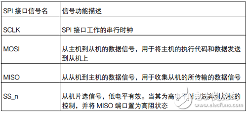

FPGA practical development skills (10)
5.5.3 SPI Serial Flash Configuration Mode