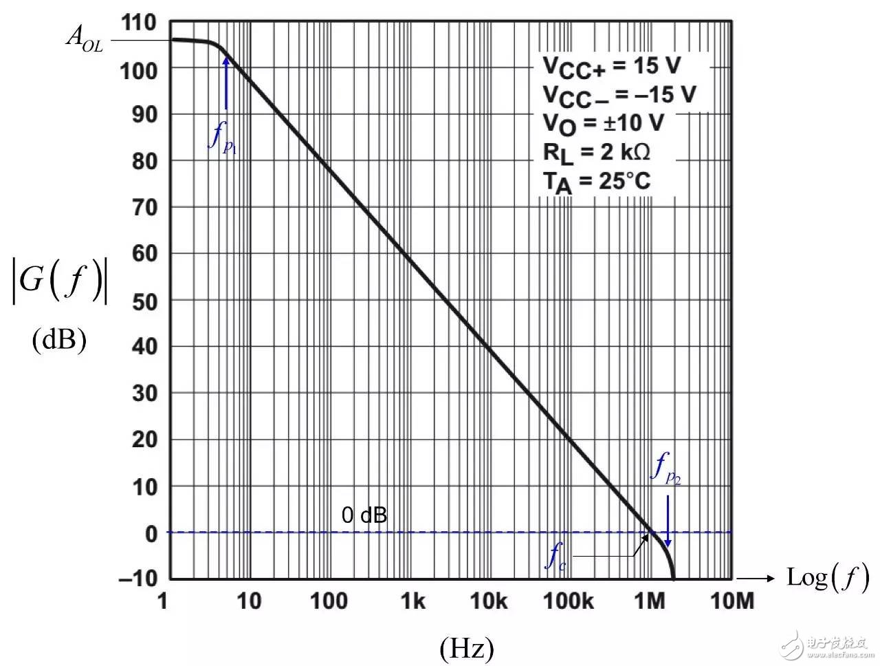
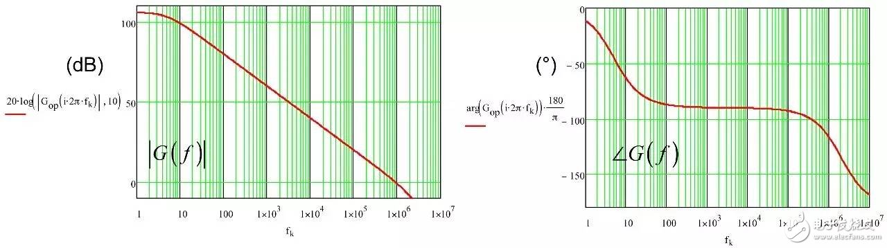
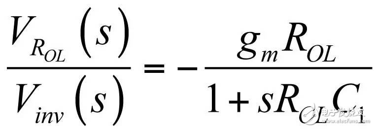
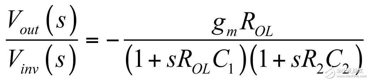
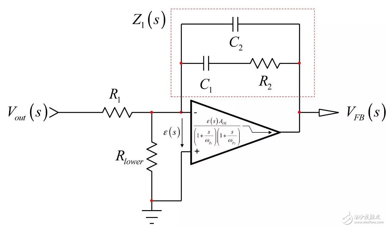
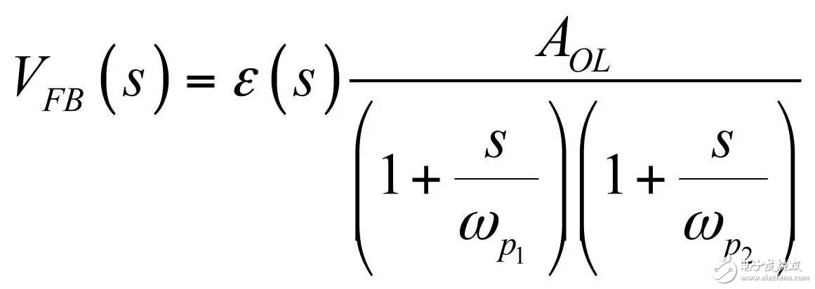
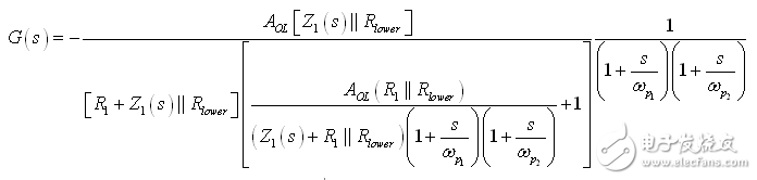
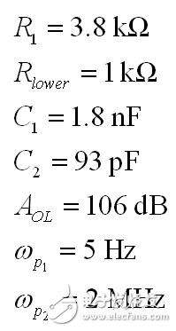
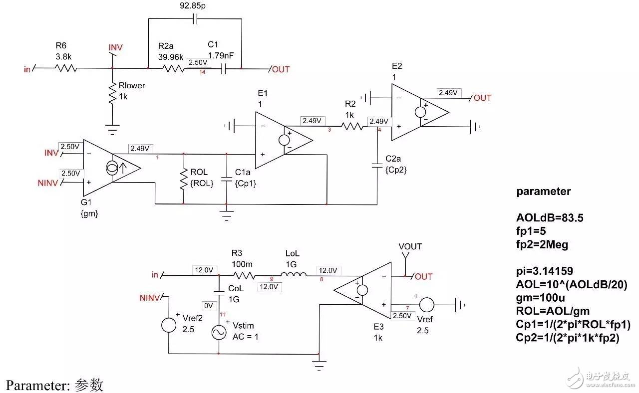
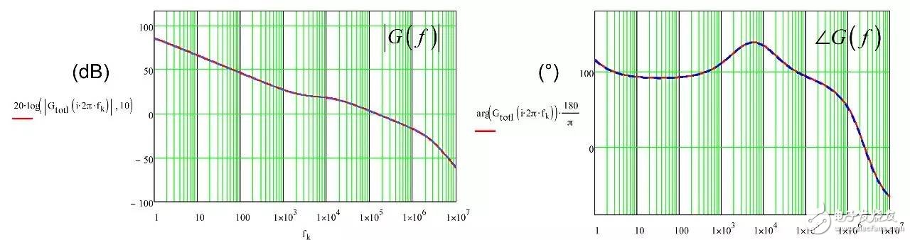
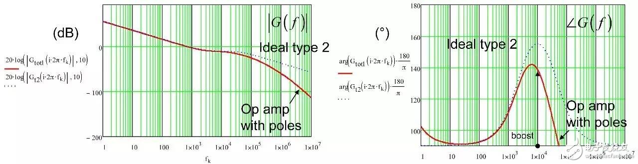
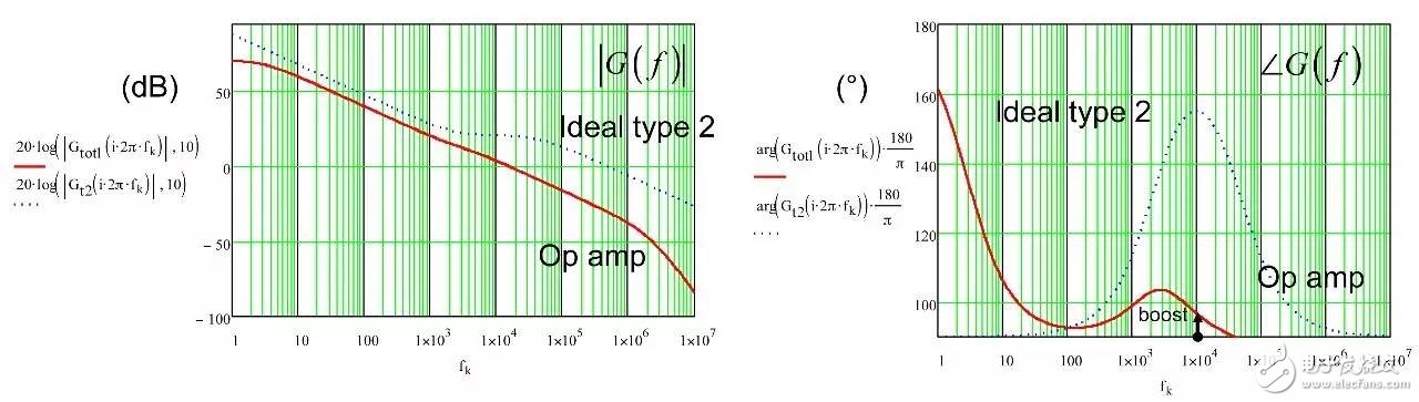
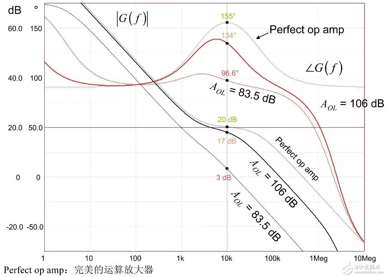
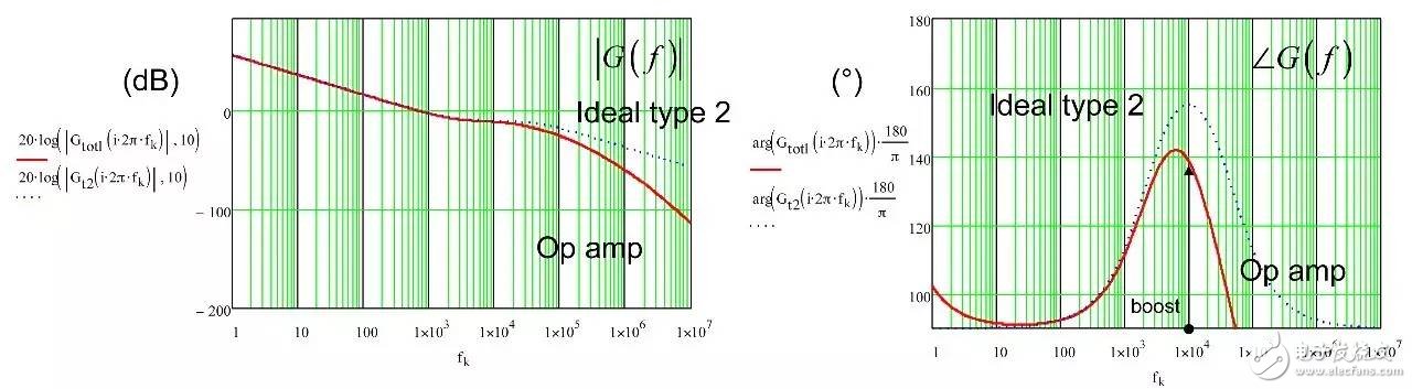
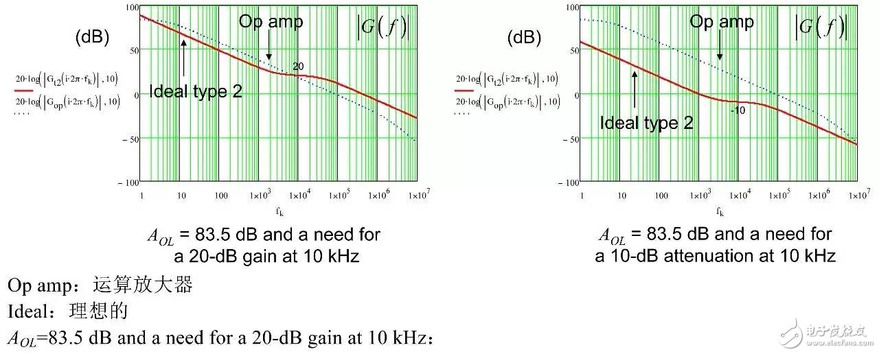
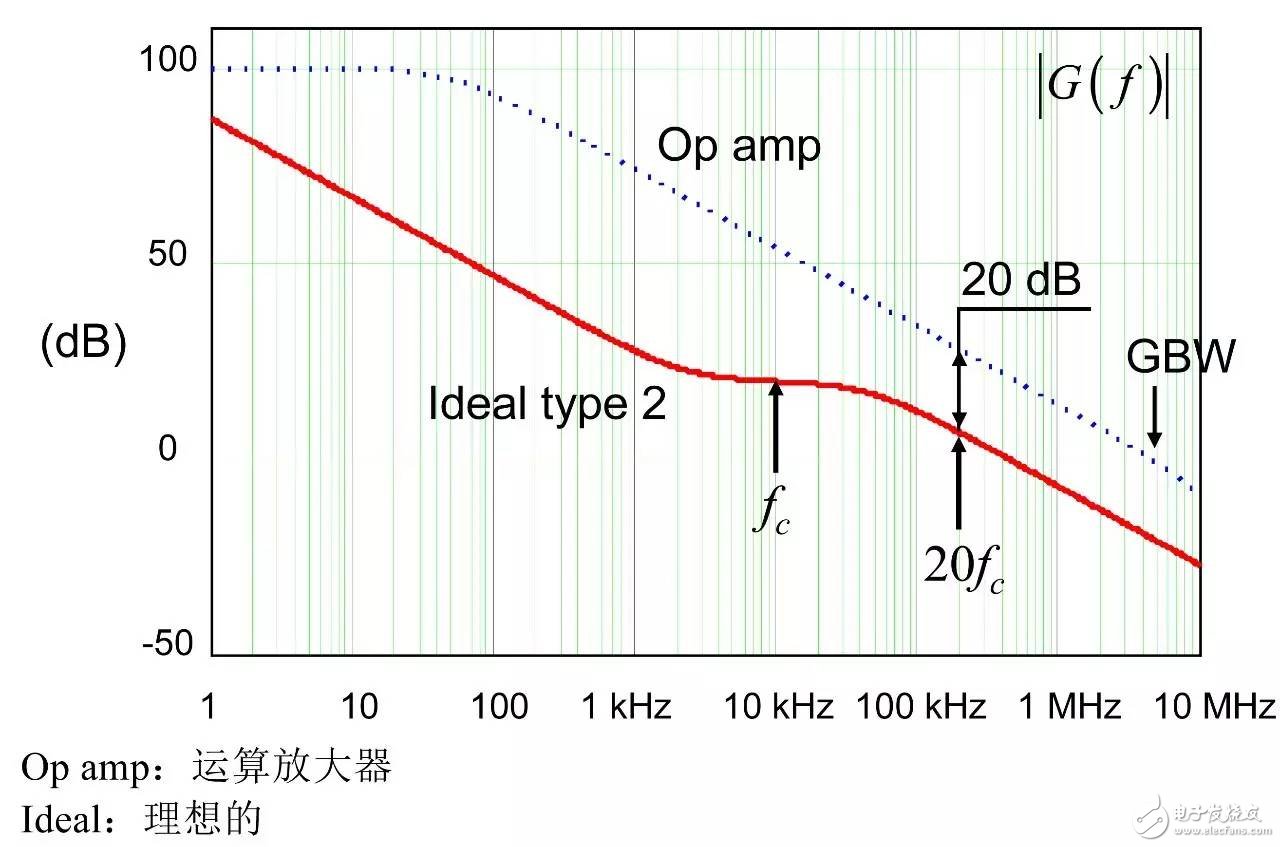
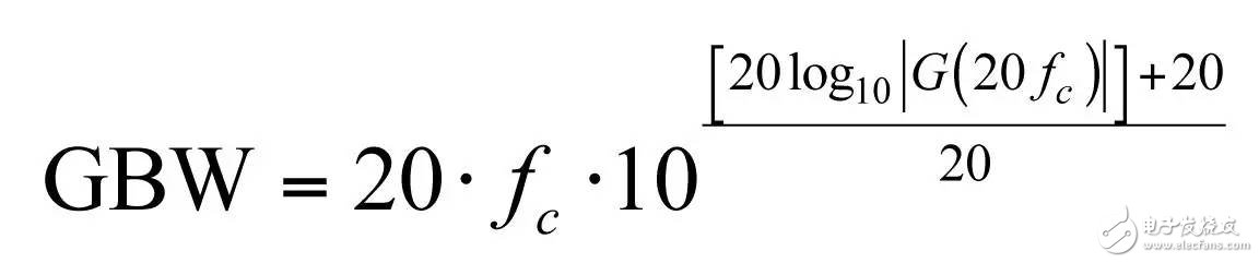
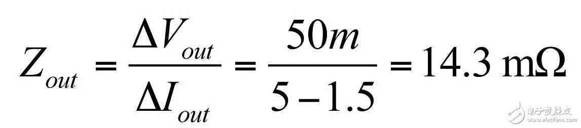
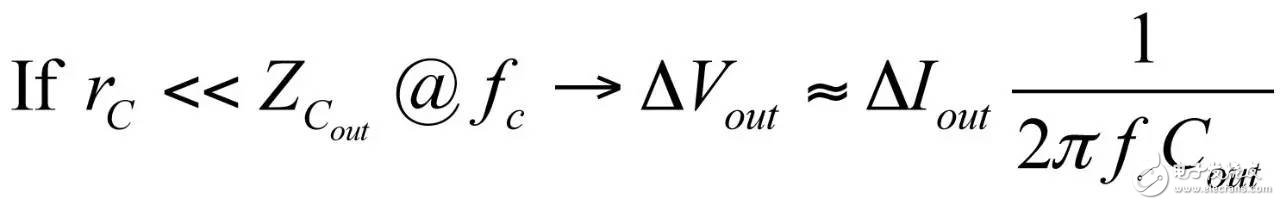
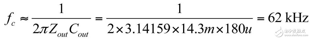
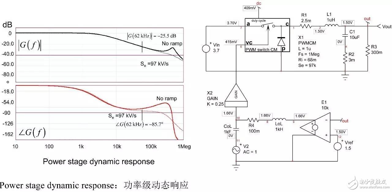
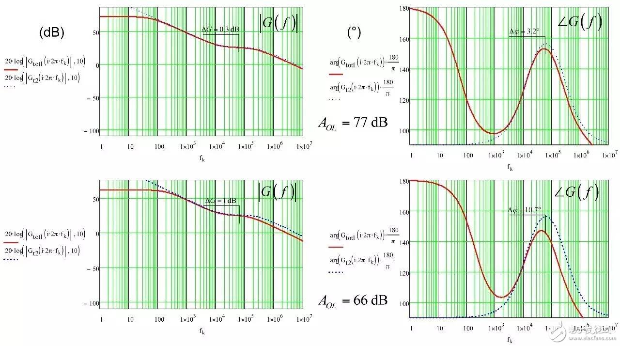
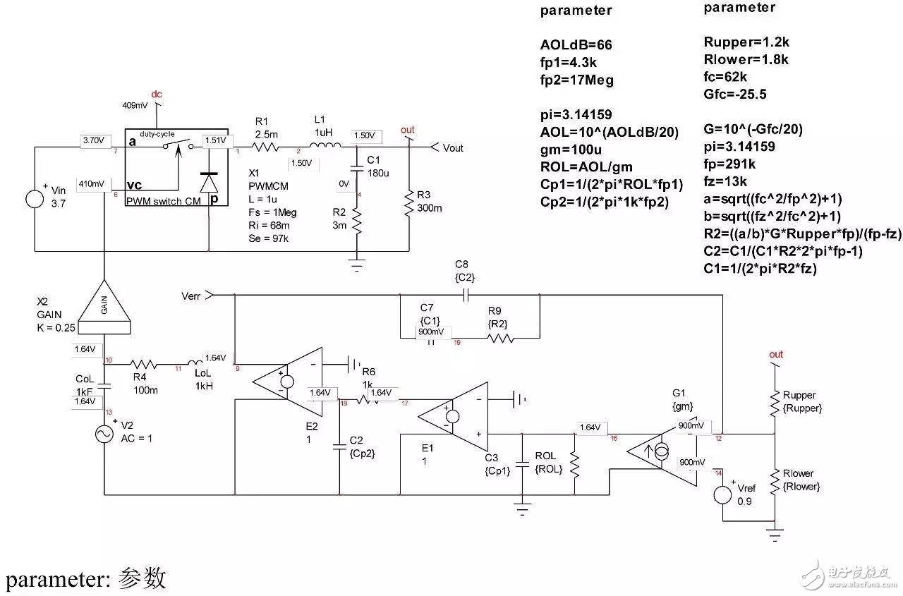
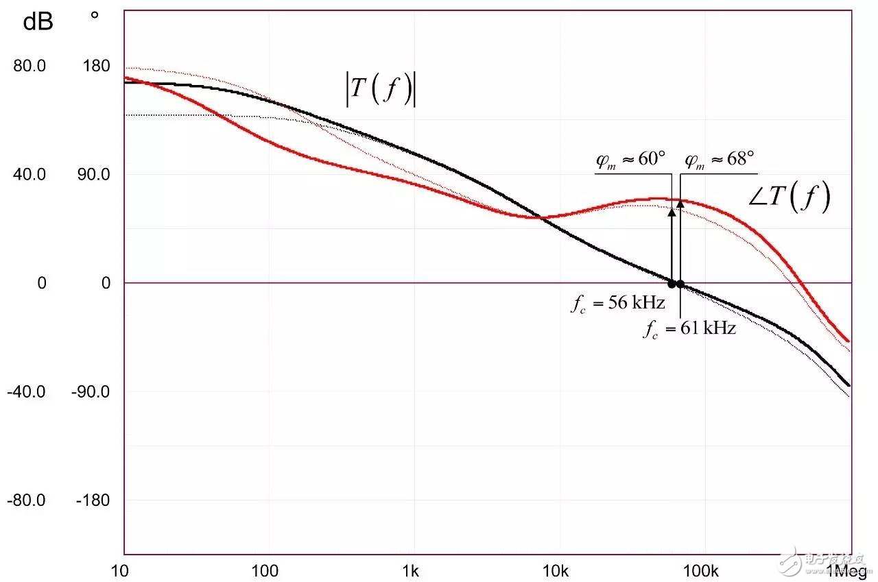
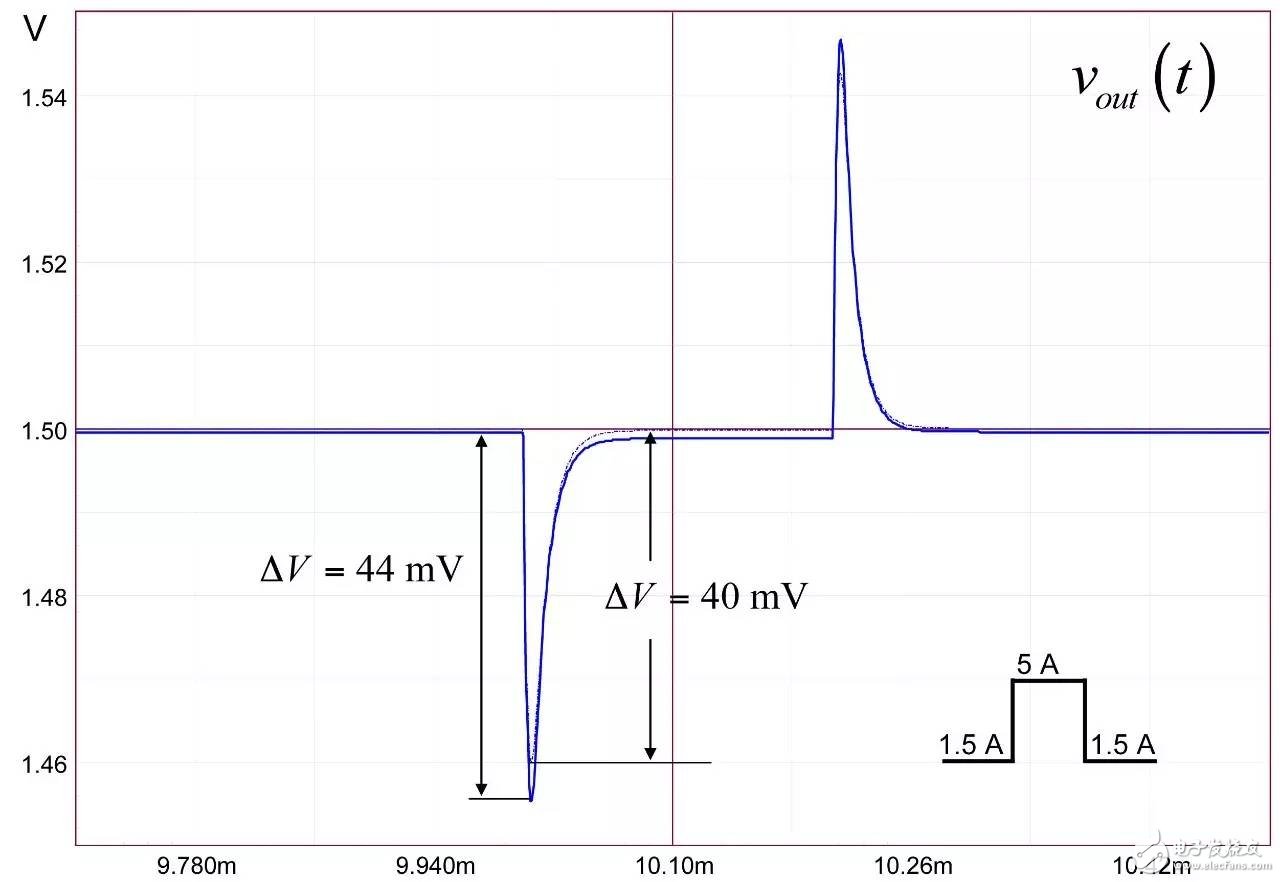
In the first part of this article, we have demonstrated the effect of an op amp on the open-loop gain AOL of a type-2 compensator . We further advance the analysis, focusing on the amplitude and phase response of the op amp, and deducing the existence of two poles, low and high. If these poles are negligible in low-bandwidth designs, but gain and phase enhancement are required in high-bandwidth systems, you must consider the distortion they introduce. In this second part, we will talk about how to determine the transfer function of the type-2 compensator due to the presence of these poles, and how they ultimately distort the performance of the filter. Two poles in an op amp For stable operation, the op amp designer implements so-called pole compensation, including placing a pole at low frequencies such that the gain at frequency f c drops to 1 (0 dB) before placing the second high frequency pole, typically at 2f c . Figure 1: The open-loop dynamic response of an op amp reveals the existence of two poles Figure 1 shows a typical μA741. You can see that the crossover frequency is 1 MHz, the low frequency pole is around 5 Hz, and the second pole appears at about 2 MHz. Note that this is a typical response with an open loop gain of A OL 106 dB. The open loop gain is not a precisely controlled parameter and it can vary significantly. The data sheet specifies that the gain is shifted from 15K (83.5 dB) to 200K (106 dB) over the entire temperature range (-55 to 125 °C), so when discrete, this curve shifts. A simple expression can be described Laplacian both poles open loop response, as shown in Figure 1: (1) Determined by the Mathcad® plot of Figure 2 : Figure 2: The op amp has a low frequency pole and the second pole is at a crossover frequency that exceeds 0 dB. A simple SPICE model of an operational amplifier We can easily build a SPICE model that mimics the frequency response of Figure 2 . As shown in Figure 3, which uses a voltage controlled current source G 1, G 1 has a transconductance g m, even after a ground resistance R OL, and then in parallel with the capacitor C 1. For R OL , the transfer function of the inverting pin V inv is simple: (2) If we now buffer the voltage and place the second pole with resistor R 2 and capacitor C 2 , we get the complete transfer function we want: (3) The component values ​​are automatically displayed on the left side of the page. Once the simulation is run, the acquired amplitude/phase map is displayed on the right. This is a simplified op amp model, but it can be used for first-order analysis. It can be later upgraded to more specific features of the model, such as voltage clamping or slew rate circuits, as described in [1]. Note the presence of LoL and CoL in the figure. Due to their presence, the op amp output voltage needs to be fixed at 2.5 V when the component is running open loop. Since there is no power rail here, we can run a simple AC analysis without considering the DC bias point. Figure 3: A simple SPICE circuit that creates an op amp with open-loop gain and two poles. However, if you are going to analyze a more comprehensive model response including the power rail, this simple circuit will prevent the IC from fluctuating up and down when you want to manually adjust the DC operating point. A LoL short circuit at the beginning of the simulation helps to adjust the operating point with E 3 and source V ref . Once the AC circuit analysis begins scanning CoL, LoL modulation block E 3, the adjustment point in turn rest. This is the usual trick to use an average model to run the open loop gain analysis while ensuring that the closed loop bias point is determined to the desired output value. This simple SPICE model will help test the mathematical expressions we analyze. Type-2 compensator has a two-pole architecture Now that we know that op amps have two special poles, we can update the sketch we originally used in the first part of this article. Figure 4 shows the newly created type-2 compensator, which now includes the internal features of the op amp. Figure 4: The update circuit takes into account the two poles present in the op amp. The output voltage V FB is the error voltage e multiplied by the open-loop transfer function of the op amp (4) In addition, the error voltage can be obtained by setting V out and V FB to 0 V using the superposition theorem: (5) If we substitute (5) into (4) and sort it out, we conclude that: (6) Z 1 (s) is equivalent to: (7) See the appendix at the end of this article to learn how to use a quick analysis technique to derive this expression in a simple step. This equation is extremely difficult to deal with, but advantageously, it is not a problem for Mathcad®. We can verify that it is correct by comparing its dynamic response to the SPICE model. We assume the following component values: Type-2 architecture using SPICE circuit 5 as shown in FIG. Figure 5: The complete type-2 SPICE model now constitutes the dynamic response of the op amp. Note that considering the 2.5 V reference voltage V ref 2 is now biased to the NINV pin, the DC bias point is set to 12 V. It is confirmed from Figure 6 that the response between Mathcad® and SPICE is the same, determining the validity of the equation. Characteristic distortion The component values ​​used in the simulation in Figure 5 are from a type-2 compensator designed to establish a 65° phase increment at a 10 kHz crossover frequency with a gain of 20 dB. If we now compare the ideal type-2 response given by equation (36) in the first part of this paper with the response of a type 2 circuit using μA741 (106 dB A OL with two poles, 5 Hz and 2 MHz), you will some differences noted, as shown in Figure 7: Figure 6: Drawing curves provided by Mathcad ® curve generated by the SPICE perfectly coincide. In this figure, we can see a slight gain deviation at 10 kHz and a difference of about 2.2 dB from 20 dB. In fact, it doesn't matter. More importantly, you achieve the desired 65° phase increment with the perfect formula. At 10 kHz, the phase increment provided by the circuit with the true operational amplifier is only 44.6° or a phase difference of 20.4°. This will correspondingly reduce the final phase margin. Figure 7: Creating type 2 with μA741 with the highest open-loop gain has caused phase delta distortion. But the back is even worse. If you consider the deviation of the open loop gain shown by the data sheet, what is the minimum size if A OL drops to 83.5 dB? Figure 8 demonstrates that the 20 dB gain difference at 10 kHz is 17 dB, while the phase increment drops to 6.7°. There is no need to explain why the stability of the system is related to the last value. The SPICE simulation of Figure 9 determines these data by three different curves acquired in the same graph. You can see the adverse effects of the open loop gain deviation. Figure 8: If the open-loop gain now drops to 83.5 dB, there is almost no improvement in phase as described in the op amp data sheet. If we change the type-2 specification now, that is, we no longer need a gain at 10 kHz, but there is 10 dB attenuation at f c , and the same phase increment is 65°, the phase increment distortion is not so obvious, open lower loop gain (see FIG. 10). Figure 9: The change in the open-loop gain of the op amp causes severe gain/phase distortion. Figure 10: If the type-2 circuit is instead amplified at 10 dB instead of at the same 10 kHz crossover frequency, the target is still not achieved, but the distortion is small. The mid-band gain obtained with this architecture is - 11 dB (relative to the -10 dB target), while the phase increment just reaches 49° (relative to the original 65° target). Type-2 response and open loop gain plotting To ensure that the compensator response is not changed internally within the op amp, the usual recommendation is to superimpose the theoretical type 2 amplitude and the op amp open-loop response [2] on the same plot. In Figure 11 , the left image corresponds to a type 2 compensator we first attempted to establish, with a 65° phase increment and 20 dB gain at 10 kHz. In this figure, the op amp amplitude intersects and contrasts with the type 2 compensator, causing the desired feature to be corrupted (final phase error is almost 60°). It is obvious at first glance that this crossover indicates that either the op amp chosen is not suitable or the target set with the type-2 compensator is too high. A OL = 83.5 dB, 20 dB gain at 10 kHz A OL = 83.5 dB, requiring 10 dB attenuation at 10 kHz Figure 11: The left image clearly shows the intersection and attenuation of these two responses. There is no intersection in the amplitude map on the right, but the final result is also distorted. The right image of Figure 11 seems to indicate that we should be able to design a type-2 circuit that has no gain but attenuation at the 10 kHz crossover frequency. But our calculations show that this is not the case, because it is determined that there is a final phase error of 17°. One of the methods in [2] suggests selecting an op amp with a gain-bandwidth product (GBW) greater than the 0 dB crossover frequency of the type 3 compensator used. However, as you can see, it does not apply to Figure 11 : On the left, the 0 dB crossover frequency of type 2 is around 400 kHz, while on the right we want to attenuate instead of gain. I propose a slightly different empirical solution where the open-loop response of the op amp must be 20 dB higher than the 20f c of the type 2 compensator. As shown in FIG. 12. The graphical approach is the first step in determining how many GBW your op amp must have in order to achieve the desired phase increment and gain target within an acceptable range. Op amp: Operational Amplifier Ideal: ideal Figure 12: As a first step, we recommend that the open-loop response of the selected op amp be at least 20 dB higher than the second -1- slope of the type 2 compensator. You first calculate the dB magnitude of type 2 at 20f c , plus 20 dB. Then you calculate the corresponding open-loop gain crossover frequency or GBW of the op amp: (8) On the left side of Figure 11 , (8) gives a GBW of 4.4 MHz, while for the second case, a GBW of 150 kHz is recommended. Apply this strategy to the first example, which results in an op amp open-loop gain of 90 dB, a low-frequency pole at 150 Hz, or an open-loop gain of 80 dB and a low-frequency pole of 450 Hz. Do not reduce the open-loop gain to less than 70 dB [ 2 ] to keep the steady-state error within an acceptable range. When applying this strategy, the midband gain is 19.5 dB and the phase increment is approximately 60°». In the second example, (8) recommends GBW 140 kHz with an open loop gain of 80 dB and a low frequency pole of 15 Hz. The mid-band gain dispersion is 0.4 dB with a phase increment of 56° or a deviation of 9°. The low frequency pole is increased to 30 Hz, the gain dispersion is reduced to 0.2 dB and the phase increment error is 4.4°. With formula (8), you can start to choose a suitable GBW for the op amp. Several conditions were observed and repeated to find the appropriate GBW. I have tried to extract the possible GBW from (6) – for example ignoring the high frequency pole effect – to match the initial perfect type 2 specific deviation, but I am not sure that a meaningful expression has been established. Once you have the recommended GBW, you can look up the op amp's data sheet and identify a suitable component. Associate A OL and low frequency poles with Mathcad® Table [ 3 ] to compare deviations from the target. Be sure to explore the minimum so that the deviation is still acceptable in the worst case. Compensation example for high frequency current mode buck converter Suppose we have designed a 5 A buck regulator to reduce the 3.7 V battery to 1.5 V with a switching frequency of 1 MHz. The output capacitor is 180μF and has an equivalent series resistance (ESR) r C of 3 mW. Suppose we want a 50 millivolt output voltage drop with a load change from 1.5 A to 5 A. Therefore the power supply output impedance must be equal to: (9) This may indicate that the impedance of the closed-loop output of the small signal at the crossover frequency f c is dominated by the capacitor impedance, which provides an ESR that is small enough: (10) From the required voltage drop, considering the 180μF capacitor and the desired 14.3 mW output impedance, we can estimate the required crossover frequency: (11) Some people will object, thinking that this is an approximate analysis of small signals, and the large signal response will be different. This is true, but experience shows that the final result is similar to the calculation. Of course, when there are ESR and ESL (parasitic inductance), the results are greatly different, but the first-order method is a meaningful starting point. In addition, analysis of this method shows that it is often ridiculous to compare the crossover frequency with the commonly proposed F sw / 5 or F sw / 10 . We chose the crossover frequency f c of 62 kHz. To compensate for this converter, we first need the dynamic response of the power stage, which is the starting point for the analysis. There are several ways: a) use the transfer-to-output transfer function H(s ) and derive the Bode plot) b) build a simulation setup with the average model c) build a prototype in the lab and extract it with a network analyzer Respond or d) Establish a switch model with Simplis® or PSIM® and extract AC response. We use the strategy b) as shown in Figure 13. Power stage dynamic response: power stage dynamic response Figure 13: Average model helps us build current mode converters very quickly From the amplitude map, we see that if we want a 62 kHz crossover frequency, the midband gain must be 25.5 dB. If our target is a 70° phase margin (pm), the phase lag (pfc) of approximately 86° at the crossover requires the following phase increment values: (12) Calculations from the Mathcad® table show that one pole is at 291 kHz and the zero is at 13.2 kHz. According to (8), a 50 MHz GBW amplifier must be selected. Looking at the data sheets for various op amps, we found that the LT1208 has a typical 7k open-loop gain (approximately 77 dB) that can be reduced to a minimum of 2k (66 dB). Its typical gain-bandwidth product is 45 MHz, which drops to 34 MHz at ±5 V supply. Therefore, the low frequency pole is located at 34 MHz / 7k, about 4.8 kHz. Figure 14: Open loop gain dispersion affects the final effective phase increment. Figure 14 shows a type-2 Bode plot of two different open loop gains. 77 dB provides 45 MHz GBW and low dispersion. When A OL drops to 66 dB (minimum specification), the gain dispersion is still acceptable, but the phase increment deviates from the target by 10.7°. Op amp in a buck converter We can now close the actual model (at least A OL with two poles) and capture the characteristics of the selected op amp to our now updated simulation schematic. Figure 15: The op amp now has two poles, low and high. From this graph, we can plot the open-loop gain T(f ) and see how the open-loop variation affects the dynamic response. The results are shown in Figure 16. As expected, there is some dispersion in the crossover frequency and phase margin. Figure 16: Dynamic response is affected by changes in open loop gain. In the worst case (66 dB A OL ), the phase margin drops to around 60°, which is acceptable (dashed line). From the simulation circuit of Figure 15 , we can run a transient load step and check the response of two different open loop gains. The results are shown in FIG. 17. Figure 17: The lowest open-loop gain has a deviation of 44 mV and the typical value results in a voltage drop of 40 mV (dashed line corresponds to 66 dB A OL ) This voltage drop is within the specification of the two open loop gain values. Of course, this is a simplified method. Considering the error voltage deviation (1.6 V) of the op amp, the slew rate must be part of the overall analysis, which affects the evaluation of the transient response. to sum up The second part introduces the impact of the op amp dynamic response on the performance of the compensator. When large bandwidths are required, you can no longer ignore these effects on the dynamic response of the compensator. You can overlay the perfect type-2 response you want with the selected open-loop amplitude map of the op amp and see if it overlaps. However, one situation we have seen is that non-overlapping ultimately leads to a significant phase incremental distortion. With a significant gap between the op amp's open-loop response and the perfect type 2 open-loop response, you can choose the gain-bandwidth product and check how it affects the desired response with a given formula. For a comprehensive stability analysis, the entire loop gain must be considered by affecting all component tolerances, including the internals of the op amp. You can do further analysis with the complete type-2 transfer function in (6). references 1. Basso, “Practical Implementation of Loop Control in Power Convertersâ€, APEC Professional Seminar, Charlotte (NC), 2015, http://cbasso.pagesperso-orange.fr/Spice.htm 2. T. Hegarty, “Error Amplifier Limitations in High-Performance Regulator Applicationsâ€, AN-1997, Texas-Instruments, May 2013, http:// 3. http://cbasso.pagesperso-orange.fr/Spice.htm 4. C. Basso, “Linear Circuit Transfer Functions – An Introduction to Fast Analytical Techniquesâ€, Wiley 2016, ISBN 978-1-119-23637-5 ↓↓↓ Read the original, see more! Capacitor For Electric Furnace Capacitor for Electric Furnace, commonly referred to as capacitors, are capacitors, expressed in the letter C.Definition 1: a capacitor, as the name implies, is a "charging vessel", a device that holds charge.Capacitor.Capacitors are one of the most widely used electronic components in electronic equipment. They are widely used in the fields of interleaving, coupling, bypass, filtering, tuning circuit, energy conversion and control.Definition 2: a capacitor consisting of any two conductors (including wires) that are insulated from each other and are very close together.
Electronic Components Capacitors,High Voltage Capacitors,Low Frequency Capacitor,Water Pump Capacitor,Capacitor for Electric Furnace YANGZHOU POSITIONING TECH CO., LTD. , https://www.pst-thyristor.com