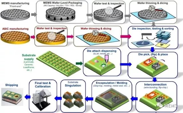
Abstract : MEMS devices are small in size and low in cost. They are the direction of future sensor development. With the advancement of MEMS technology, inertial MEMS sensors and medium-angle frequency sensors have high-resolution and low-cost inertial components for measuring the yaw angle of missile attitude. And rotate the scroll rate. In MEMS devices, packaging technology is of utmost importance. In addition to integrated technology, the robust inertial MEMS devices have become another core. We have conducted research on packaging technologies to improve the reliability of MEMS devices. MEMS device packaging technology follows the trend, its preparation process and equipment are quite mature, and the application of MEMS devices is not many, and there is no large-scale promotion. Because the packaging technology of MEMS devices does not reach a very high level, the packaged devices are not of good quality. The immaturity of MEMS device packaging technology largely limits the development of MEMS commerce. 1 MEMS Overview MEMS (micro-electro-mechanical systems) are relatively independent intelligent systems. They are small in size, only a few millimeters or even smaller, and consist of three major components: sensors, actuators, and micro-energy. MEMS design includes a variety of disciplines, mainly physics, chemistry, materials engineering, electrical engineering and a series of disciplines, MEMS applications in many areas, automotive electronics, computer, consumer electronics, network communications, these four categories Is the most common area. MEMS process has many similarities with traditional IC process. MEMS draws on IC process, such as photolithography, thin film deposition, doping, etching, chemical mechanical polishing process, etc. For the millimeter or even nano-level processing technology, the traditional IC The process cannot be achieved and must rely on micro-machining to perform fine processing to achieve the desired structure and function. Micromachining technology includes silicon micro-machining technology and surface micro-machining technology. The body processing technology refers to a process of etching a silicon substrate along the thickness direction of a silicon substrate, and is an important method for realizing a three-dimensional structure. Surface micromachining is the use of thin film deposition, photolithography and etching processes, by depositing a structural layer film on the sacrificial layer film, and then removing the sacrificial layer to release the structural layer to achieve a movable structure. 2 MEMS Device Packaging Advantages Micro-electro-mechanical systems are based on the integration of functions on the chip, the size is generally below the millimeter, the production process is more precise, the higher technology is needed, the MEMS has been applied as early as abroad, China started late, and investment in MEMS gradually Increased, the market share is increasing. The emergence and development of MEMS are the result of modern scientific innovation thinking and the evolution and revolution in micro-scale manufacturing technology. MEMS is the most widely used in the field of sensors. Because of its small size, light weight and low cost, MEMS products are rapidly increasing in demand in many fields, and they are rapidly growing in consumer electronics and medical fields. A large number of MEMS products have been discovered. MEMS has the following five characteristics: 2.1 Miniaturization MEMS devices are generally "small," whether they are in terms of volume, weight, energy consumption, or cost. They all belong to the "mini" series, and they have high work efficiency and short response times. 2.2 Wide range of materials and excellent performance Most of the raw materials for integrated circuits and MEMS are silicon, which can be extracted from silicon dioxide through chemical reactions. Silica is the main component of sand, and raw materials are everywhere. In addition, the hardness of silicon is comparable to that of iron, and its density is small. Similar to aluminum, its thermal conductivity is strong. 2.3 Mass production Complete MEMS are fabricated on a single piece of silicon at the same time. Large production can increase production efficiency and save a lot of costs. 2.4 Integration A system composed of various sensors or actuators with different functions forms a microactuator array and a microsensor array, and can also combine various functional devices to form a complicated microsystem. The combination of micro-actuators, sensors, and microelectronic devices creates MEMS with high reliability and stability. 2.5 Interdisciplinary MEMS design knowledge is extensive, multidisciplinary knowledge intersects, MEMS technology becomes extremely complex, involves all aspects of knowledge, MEMS devices draw on many modern scientific and technological development achievements. 3 MEMS Device Packaging Technology 3.1 Flip Chip Technology Flip-chip bonding places the chip face down and then packages it with the package substrate. This benefit is reflected in the direct connection of the chip and the substrate, the silicon chip can be directly inverted on the PCB, and then I/O from the periphery of the silicon. Leading out I/O directly, does not need to connect from an interface above again, has shortened the length of the interconnection greatly, then reduced the delay, raised the running speed, reached the ultimate goal and improved the electric energy sex. Obviously, for this type of connection, the space can be utilized to the maximum extent, and the volume will not be too large because of the excessive connection. On the contrary, the effect of flip-chip is almost the same as that of the original chip, which greatly improves the operating efficiency. . In all surface mount technologies, flip-chips can reach the smallest and thinnest packages, resulting in a smaller device size after the entire package. Because the bumps fill the entire die, the interconnect density of the I/O is also greatly increased, which speeds up the input and output efficiency, shortens the connection time, shortens the signal transmission time, and greatly improves the electrical performance. If this technique is applied in a micro-microphone, it is necessary to shorten the lead between the amplifier and the microphone in order to reduce signal crosstalk and lead inductance. In order to achieve this goal, the micro-microphone MEMS chip and the amplifying circuit need to be packaged together. Such a device package needs to adopt the flip-chip welding technology, and the reduced package volume can also support some other uses. The micro-microphone after being encapsulated by the MEMS device has the characteristics of low power consumption and high sensitivity, which greatly improves the effect of the microphone. Compared with the traditional electret microphone, the micro-microphone is much cheaper. MEMS microphone manufacturing, packaging, and testing processes 3.2 Multi-chip component technology Multi-chip modules (MCMs) are system-level packages and represent a major breakthrough in electronic packaging technology. MCM refers to a package that contains two or more chips that are interconnected by a substrate and collectively form a package of the entire system. It also provides signal interconnection, I/O management, thermal control, mechanical support, and environmental protection for all chips in the assembly. 3.3 Multi-chip package Multi-chip packaging is another trend in MEMS packaging. Compressing the volume of the entire device, adapting to miniaturization, shortening the distance between the signal and the actuator, and reducing various influences caused by signal and external interference, the MEMS chip and the signal processing chip are placed in the same package. Based on the use of ceramic substrates, the sensors were mounted together using wire bonding technology to package the substrates, and the MEMS package was successfully completed. MCM offers a unique approach to integrating and packaging MEMS devices that can simultaneously support multiple chips on the same substrate, without changing the manufacturing techniques of MEMS and circuits, and its performance can be made without compromise. optimization. The replacement of the traditional single-chip package structure with the MCM technology-based MEMS package has no problem, and the device's performance and reliability have also been significantly improved. For example, the packaging of accelerometer sensors that control circuits and MEMS chips are mounted on a single substrate produced by Shanxi Ketai Co., Ltd. utilizes this packaging technology to improve the reliability and packaging density of packages and improve production efficiency. The rate of mass production. From the perspective of various technical advantages, it is feasible to complete the interconnection of MEMS chips and substrates. 4 Conclusion The development of MEMS packaging technology draws lessons from IC packaging experience and reduces the production cost. In the initial stage of chip structure design, the idea of ​​modeling is used to simulate the package and find suitable materials and processes. With the development of MEMS packaging technology, the technological process will only become more and more complicated and more and more diversified. It will accelerate the research of MEMS packaging technology and provide high-quality products. Company Introduction: Naturehike Products Co., Ltd. is a leading outdoor gear and equipment manufacturer based in China. The company is committed to providing high-quality and affordable outdoor gear to customers around the world. With a focus on innovation and design, Naturehike Products Co., Ltd. has become a trusted brand among outdoor enthusiasts. The company's products are designed to withstand the rigors of outdoor activities and are tested in extreme conditions to ensure their durability and performance. Naturehike Products Co., Ltd. is dedicated to promoting the outdoor lifestyle and helping people connect with nature.Company Introduction: Naturehike Products Co., Ltd. is a leading outdoor gear and equipment manufacturer based in China. The company is committed to providing high-quality and affordable outdoor gear to customers around the world. With a focus on innovation and design, Naturehike Products Co., Ltd. has become a trusted brand among outdoor enthusiasts. The company's products are designed to withstand the rigors of outdoor activities and are tested in extreme conditions to ensure their durability and performance. Naturehike Products Co., Ltd. is dedicated to promoting the outdoor lifestyle and helping people connect with nature.Company Introduction: Naturehike Products Co., Ltd. is a leading outdoor gear and equipment manufacturer based in China. The company is committed to providing high-quality and affordable outdoor gear to customers around the world. With a focus on innovation and design, Naturehike Products Co., Ltd. has become a trusted brand among outdoor enthusiasts. The company's products are designed to withstand the rigors of outdoor activities and are tested in extreme conditions to ensure their durability and performance. Naturehike Products Co., Ltd. is dedicated to promoting the outdoor lifestyle and helping people connect with nature. Enzyme Cream,Whitening Slimming Enzyme Cream ,Meal Replacement Diet Enzyme Cream ,Conditioning After Surgery Enzyme Cream Bossgoo(China)Tecgnology , https://www.cn-gangdao.com