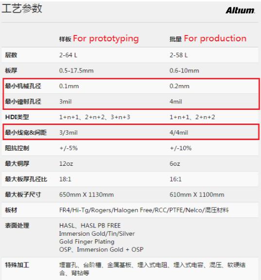
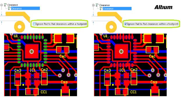
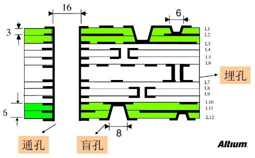
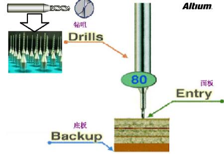
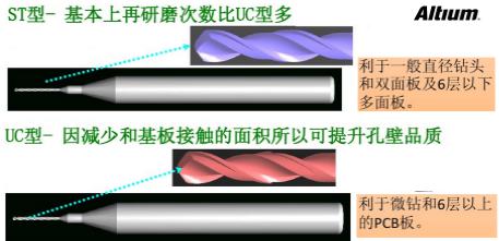
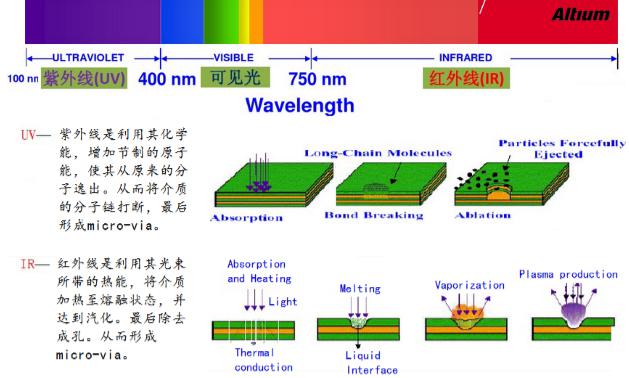
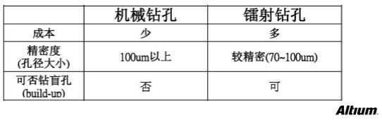
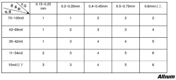
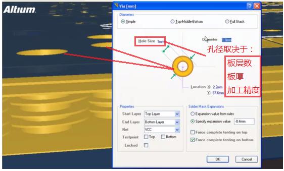
In PCB design, Design Rule design rules are the key to the success or failure of a PCB design. All designer's intentions, the functional embodiment of the design are driven and realized through the soul of design rules. The meticulous definition of the rules can help designers get the job done in PCB layout and wiring, save engineers a lot of energy and time, help designers achieve excellent design intent, and greatly facilitate the design work. After the design data is transferred from the schematic phase to the PCB design phase, when designing the PCB design layout, it is necessary to define the design rule Design Rule in advance. Subsequent entire PCB designs need to follow the rule definition. Including the most basic electrical rules (pitch, short-circuit open circuit), wiring rules (line width, trace style, via pattern, fanout, etc.), plane rules (power ground plane connection, copper connection); and others Common auxiliary rules such as layout rules, manufacturing rules, high-speed design rules, signal integrity rules, etc. After the rule-driven design is completed, you can also conduct a rule check Design Rule Check to revisit your design to see if there is any violation of the rule and improve and perfect it. Ultimately, we design an outstanding work that fully meets the definition of the rules and satisfies the design intent. Relative to the PCB manufacturing design rules are particularly relevant. If the design rules do not meet the requirements of the PCB process manufacturing, it will not only affect the function of the product, it will be even simple, and it will not be able to process the design intent of the engineer. Therefore, when defining the design rules, it is important to understand the requirements of the downstream manufacturing manufac- turer for the design process. What are the accuracy requirements of the PCB manufacturing process?       The following figure shows the process requirements of a PCB board manufacturer. Including the number of circuit board layers, thickness, aperture, minimum line width, copper thickness and other basic parameters; also includes special requirements such as sheet type, surface treatment, and special processing. In general, when PCB is processed, the proofing process is divided into tests, and the final shaped batch product is processed. For designers, what is practical and needs to be strictly followed is the process requirements for mass product processing.       The most basic and most important of the manufacturing requirements related to manufacturing accuracy is the line width and minimum aperture. That is, the processing plant can handle the smallest and finest line width and the smallest hole. If the line width does not meet the requirements in the design, it will not be processed correctly if it is too thin. Line spacing accuracy also affects whether the text pattern on the silk screen is clear. If the aperture is too small, there is no corresponding drill bit to support it. The size of the drill bit corresponding to the smallest aperture also affects the tolerances of various types of plate-shaped cutting such as mechanical holes and mounting holes. Line Width and Aperture Rule Settings Considerations    This article will show you how to set the line width and aperture rule that meets the requirements and meets the design intent in terms of PCB manufacturing accuracy according to PCB manufacturing process requirements. Minimum line width/space 4mil     In PCB design, the highest precision that can be supported by batch processing is line width 4mil. That is, the width of the wiring must be greater than 4mil, and the spacing between the two lines also needs to be greater than 4mil. Of course, it is only the minimum limit of line width. In actual work, the line width needs to be defined as different values ​​according to design requirements. For example, the definition of the power network is wider, and the definition of the signal line is more detailed. These different requirements can be defined in the rule Design - Rules - RouTIng - Width different line width values ​​for different networks, and then apply the priority based on the importance of setting rules. Similarly, for line spacing, the electrical security spacing between different networks is defined in the rule page Design - Rules - Electrical - Clearance, and of course the line spacing. There is also a special case. For high density pin components, the spacing between pads within the device is typically very small, such as 6 mils. Although meeting the minimum line width or manufacturing requirements with a pitch greater than 4 mils, it may not be suitable as a design PCB. Rule design requirements. If the minimum safety spacing setting for the entire PCB is 8 mils, then the pitch of component pads significantly violates the rule setting. When the rule is checked or edited online, it is always highlighted in green to show the violation. This kind of violation obviously does not need to be dealt with. We should correct the rule setting to eliminate green highlighting. In the original approach, separate security spacing rules for the device were defined using the query language and set to high priority. In the new version, only a simple check option is needed to solve this problem. Ignore Pad to Pad clearance within a footprint is ignored. As shown below.       Checking with this option is very easy. You don't need to use the Query statement InComponent('U1') as it was, then set its minimum security spacing to 6mil and set it to the highest spacing priority. 2. Minimum mechanical aperture 0.2mm (8mil) Minimum laser aperture 4mil       Drill holes are inevitably used in PCB design. In terms of setting up the design rules and even the specific drilling operations, what kind of hole (through hole, blind hole, buried hole, or back hole?) and how many holes you drill should be drilled, you have a good idea. Yet? Will you be able to see how many holes are drilled by others and how many holes are drilled, or are you willing to fill in a size to meet the convenience of board layout and alignment? The hole type is shown in the figure below. In general, less complicated designs, through-holes are often used in designs where there are not many plate stacks. In the complex design, especially the multilayer board, high speed and high density design, PCB wiring space requirements are very high, according to the actual need to set blind or buried holes. Of course, the blind buried hole is more complex than the through hole in the manufacturing process, and the manufacturing cost will increase accordingly. The difference between mechanical drilling and laser drilling       First understand the process of drilling. As shown in the figure below, drilling is performed using drill sizes of different specifications. If the size of the via hole in your design is not the same as the current drill size of the processing plant, then the drill bit closest to your design value will be selected to drill. The Entry panel is used to protect the drill bit and countertop, reducing burrs and lowering the temperature of the drill bit. The Backup backplane is used to protect the board surface from indentation, prevent skidding and reduce burrs. Drills that are mechanically drilled are usually ST type and UC type. In general, UC type is more accurate than ST type drilling.       Laser drilling is generally used for micro-vias. With the trend of micro- and high-density interconnects for PCBs, more and more board fabrications use vias to achieve high-density interconnects. The hole capacity of traditional mechanical drilling is almost to the limit. With the development of blind hole design, the reliability of high density needs new processes to improve, and laser drilling has emerged. The following figure shows the laser drilling method.        Therefore, the difference between mechanical drilling and laser drilling is as follows: The accuracy of laser drilling is much higher than that of mechanical drilling. Therefore, the minimum mechanical drilling hole size should not be less than 0.2mm (8mil) in the regular setting. The minimum laser aperture can not be set less than 4mil in the rule. 3 is provided with an aperture plate layer thickness, layer number relationship       The size of the aperture is determined first according to the accuracy required for the board, the thickness of the board, and the number of laminates, etc., when the minimum process requirements are met. The relationship between them is as follows:      Therefore, when setting the aperture size, refer to the table above to set the appropriate size according to the plate thickness, stacking number, etc. It is also possible to define the size of a suitable drilling hole size based on the entire plate thickness size by the following simple plate thickness/aperture ratio. Cross-over Ethernet Cable is also called cross wire. When the crystal head made by different standards at both ends of the wire is T568A at one end and T568B at the other end, then it is the cross wiring mode.
The crossover cable is used to connect ADSL modems to the HUB HUB (related to the MODEM design, but not all), the HUB to HUB connection without a stage port, and the two computers to each other directly through the network card.The production method is basically the same as above, except that the online order is different from 568B, which adopts the method of exchanging 1-3,2-6, that is, one end is made with 568B and the other end with 568A.
Crossover Lan Cable,Crossover Network Cable,Ethernet Crossover Cable,Lan Cable Cross Connection Shenzhen Kingwire Electronics Co., Ltd. , https://www.kingwires.com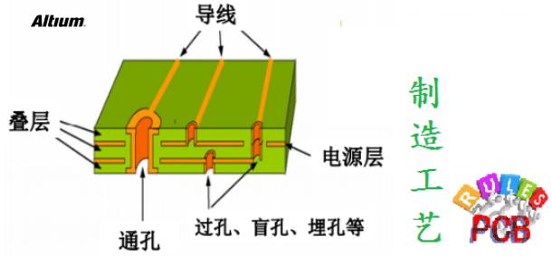

")