In the case of the competition between 182mm and 210mm and the decline of 158mm, Sunket still retains a 158mm production line to meet the needs of customers.
Their exceptional low-light and high-temperature performance enables more flexibility in installation and mounting. Mono PERC may not be suitable for all types of solar projects. However, they are optimal for residential rooftop installations, where faster ROI and lower installation costs are the driving factors.
The standard monocrystalline cell presents a uniform back surface field (BSF), whereas the mono PERC Solar Cell presents local BSF atop passivation and SINx capping layers, which significantly improves the capture of light and electrons.
Your solar panels need to be exposed to sunlight in order to produce power. However, unless you live somewhere with high amounts of smog, dust, dirt or sand blowing around, Solar Panel cleaning is generally not necessary.
158mm Solar Panel,158.75mm Solar Cell,158 Solar PV Module,6 inch Solar Panel,Solar PV Module Wuxi Sunket New Energy Technology Co.,Ltd , https://www.sunketsolar.com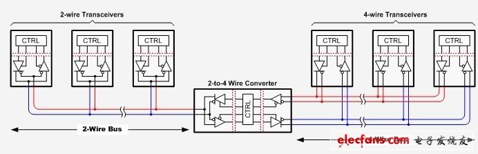
Figure 1 2-4 line converter ensures versatility between half-duplex and full-duplex systems
In order to make the converter run independent of the data rate, we control the turn-on and turn-off of the converter driver and receiver through the logic state of the bus. The bus driver is at every bit interval, allowing the converter to operate independently of the signal data rate.
Simple control logic ensures that drivers D1 and D2 are only enabled by logic low activation of the opposite receiver (ie R1 or R2) output. Because there is a bus fault protection voltage of VFS > 200 mV at the receiver input, both receiver outputs are logic high during bus idle. The inverter gate reverses the logic high to a low state and enables the receiver while the driver is turned off.
In the half-to-full duplex direction ( Figure 2 : left to right), the negative bus voltage at the R1 input activates driver D2 and uses a low state for the driver input. D2 responds by driving the transmission bus with a negative output voltage. When the bus voltage at the R1 input becomes positive, D2 immediately expires. However, its output is high because the fail-safe bias resistor RFS forms the bus voltage VFS.
(Note that during the entire run, the output of R2 is always high, ensuring that R1 remains active and D1 remains inactive.) 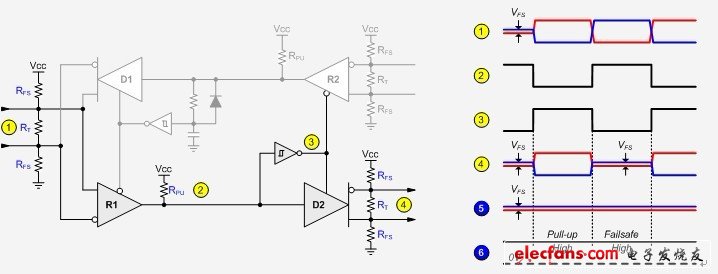
Figure 2 Half-duplex to full-duplex converter timing
In the full-to-half duplex direction (Figure 3: from right to left), the negative bus voltage at the R2 input activates driver D1 and applies a low state to the driver input. D1 responds by driving the two-wire bus with a negative output voltage. When the bus voltage at the R2 input becomes positive, D1 expires after a delay time. During this delay time, D1 uses a negative voltage to drive the bus before high impedance occurs to prevent switching transients at the R1 output.
We recommend that the minimum delay time generated by the RD?CD time constant should be 1.3 times the maximum propagation delay of the driver to compensate for component values, inverter thresholds, and supply voltage tolerances. The required RD value can be determined by Equation 1 for a given capacitance condition: 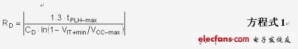
Where tPLH-max is the maximum low-to-high propagation delay of driver D2, VIT+min is the minimum positive input threshold of the Schmitt-triggered inverter, and VCC-max is the maximum supply voltage.
After D1 fails, the bus voltage VFS formed by the fault protection bias resistor RFS has its output still high. When the bus voltage at the R2 input returns to negative, the CD is immediately activated due to the rapid discharge of the CD through the discharge diode DD. The timing diagram shown in Figure 3 shows a remote receiver on the half-duplex bus (here denoted by R ) that converts the negative bus voltage to a low bit. A high bit consists of a low main drive positive bus voltage and a residual fault protection voltage VFS. 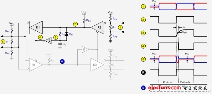
Figure 3 converter timing from full duplex to half duplex
The last converter design shown in Figure 4 uses two full-duplex transceivers: one configured as a half-duplex transceiver and the other in full-duplex mode. The converter has a data rate of up to 200 kbps and is powered by a single 3.3 V supply. Table 1 shows the bill of materials (BOM) for this circuit.
Signal Chain Basics: How to Design a 2-4 Line Converter for RS-485
Multipoint data communication networks, such as Profibus, Modbus, and BACnet, typically require RS-485 dual-wire, half-duplex bus systems and four-wire, full-duplex bus system versatility. These systems can be extended to hundreds of meters in length and withstand large ground potential differences (GPD). These potential differences can exceed the common-mode voltage range of the transceiver and cause damage to the device. To eliminate GPD, we use an electrically isolated transceiver to isolate the control electronics of the bus node from the actual transceiver stage of the connected bus. Figure 1 shows a block diagram of a hybrid network using a 2-4 line converter.
How long do solar panels last?
about 25 to 30 years
But the solar panels generating that power don't last forever. The industry standard life span is about 25 to 30 years, and that means that some panels installed at the early end of the current boom aren't long from being retired.