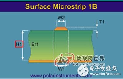
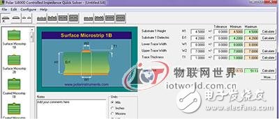
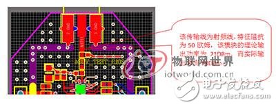
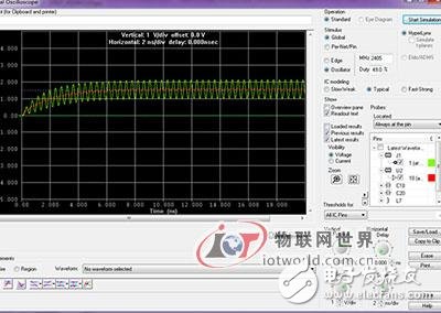
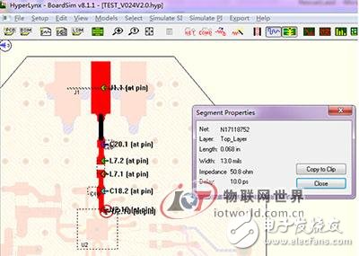
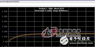
Since Marconi invented the radio, wireless communication technology has been moving toward increasing data rates and transmission distances. The currently widely researched ZigBee technology is a low-rate wireless communication technology that provides people with low cost, low complexity, low cost and low power consumption. This wireless technology is widely welcomed for its low power consumption, reliable data transmission, large network capacity, good compatibility, high security performance, low cost and short delay. The ZigBee name is derived from the communication method used by the bee colony to survive and develop. The bee uses the dance of the ZigZag shape to inform the location, distance and direction of the found food source as the name of the technology. ZigBee, formerly known as "HomeRF Lite", "RF-EasyLink" or "FireFly" radio technology, is now collectively known as ZigBee technology. At present, ZigBee technology is widely used in Internet of Things systems, such as smart home, coal mine monitoring, elevator Internet of things, etc. The quality of ZigBee circuit design directly affects the stability and reliability of IoT system operation. ZigBee-compatible products work on IEEE802.15.4 PHYs, and their frequency bands are free and open, 2.4GHz (global), 915MHz (US) and 868MHz (Europe). The ZigBee product used in this paper uses a working frequency band of 2.4 GHz, which is many times higher than the traditional signal transmission speed, so the design requirements of the board are also much more complicated. With the traditional PCB design experience can not meet the requirements of the RF board, we need to adopt a new technology for RF circuit board - signal integrity simulation technology. 1 microstrip line impedance matching simulation and calculation 1.1 Characteristic impedance definition For high-speed circuits, when we discuss transmission lines, we must consider not only the new frequency factors introduced by high-speed signals, but also the different circuit structures formed by high-speed signal transmission. In theory, the transmission line is composed of the signal line that transmits the signal, that is, the microstrip line A in the figure, and the signal constitutes a reference return path. This structure is determined by the characteristics of the signal on the transmission line. Again, we are not talking about the DC field steady-state electrostatic field analysis on the wire. The problem we face is the alternate process of instantaneous electromagnetic field during high-speed signal transmission. Therefore, please pay special attention to the fact that it is not only the common ground plane that can provide the return path for the signal line. Any conductor that can establish an electromagnetic field connection with the signal line can establish a transmission line with the signal line. The object of our study is the pair of transmission line structures that are most effective in providing the return path among all of these transmission line structures. As shown in the following figure, for the transmission line of high-speed signals, the propagation of energy depends on the alternating change of the electromagnetic field on the transmission medium, then its transmission path includes: the microstrip line itself, the return path, and the micro The medium between the line and the return path. Therefore, for a particular transmission line, a dual-port network is formed between the signal line and the return path. The impedance is the combined result of the various factors that make up the equivalent circuit. After understanding such a signal transmission structure, it is not difficult to understand the difference between the transmission line impedance and the resistance. When it comes to the impedance of the transmission line, it must not be replaced by the resistance of the conductor A. It is essentially the relationship between the electric field established at a certain point in the transmission medium and the current flowing through the point. The electric field on the transmission medium. So when it comes to the impedance of the transmission line, the reader must establish the structural concept of "two conductors", not just the obvious microstrip line A. The reference reflow path is missing, and a single microstrip line A cannot establish an electric field. When the signal is transmitted on the transmission line, each equivalent circuit that transmits a minimum unit forward must establish a corresponding electromagnetic field on the path that passes, and a certain current flows through the equivalent circuit. The impedance of the equivalent circuit of this smallest unit, relative to the transmission line, is the instantaneous impedance at this moment. If the instantaneous impedance is exactly the same when the signal is transmitted on this transmission line, then the instantaneous impedance is defined as the characteristic impedance of the transmission line. 1.2 microstrip line concept In a PCB, a microstrip line is a transmission line that separates a wire from a ground plane by a dielectric. The thickness of the printed trace, the width and the thickness of the dielectric between the trace and the ground plane, and the dielectric constant of the dielectric determine the characteristic impedance of the microstrip line. The geometry of the microstrip line is shown in Figure-1, and the width of the tape is printed on a thin grounded dielectric substrate. figure 1 W1 and W2: the width of the lower surface of the transmission line; T1: the copper thickness of the transmission line, such as an ounce; H1: the thickness of the medium; The bottom copper is the reference plane of the transmission line, which can be a ground plane or a power plane. According to the "IPC-2141" specification, the recommended microstrip line parameters are calculated as follows: Equation-1 Microstrip line characteristic impedance calculation formula: Z0 = {87/[sqrt(Er+1.41)]}*ln[5.98H/(0.8W+T)] Formula-1 Where W is the line width, T is the copper thickness of the trace, H is the distance from the trace to the reference plane, and Er is the dielectric constant of the PCB material. This formula must be at 0.1 "(W/H) "2.0, and 1 "(Er)" 15. The larger the width W of the microstrip line, the lower the characteristic impedance Z0 of the microstrip line. The approximation formula has a higher precision when the microstrip line width W is much larger than the medium thickness t, otherwise it needs to be corrected. When W is equivalent to t, the error is about a few percent to a few tenths of a percent. The width W of the microstrip line is much larger than the thickness t of the dielectric, which is what the current PCB process can achieve. However, for PCB design engineers, it is very inconvenient to control the characteristic impedance of the PCB microstrip line by relying on the above formula. In previous years, there was no professional characteristic impedance simulation software. When the PCB needed impedance matching, the engineer took a lot of time to calculate the model of the microstrip line. Later, the birth of POLAR SI8000 software brought great convenience to impedance matching calculation. At present, more than half of PCB manufacturers around the world use this software to calculate the characteristic impedance of PCB transmission line. The software is not only simple to use, but also has high impedance matching accuracy. The software provides a variety of PCB transmission line models. This article only describes how to design the characteristic resistance of the ZigBee module microstrip line with SI8000. Because the model of ZigBee RF signal transmission line is microstrip line and the characteristic impedance is 50 ohms, according to the actual process requirements of PCB manufacturers, if the thickness of copper is 1 ounce, only the width of the microstrip line can be calculated by SI8000 software. The characteristic impedance of the microstrip line is controlled. Specific steps: Run SI8000 software, the interface is as shown in Figure-2 below, and the model for selecting the microstrip line is: Surface Microstrip 1B. The thickness H1 of the first layer to the second layer is 4.5 mil, the width of the upper and lower lines of the microstrip line is different (W1-W2) 1 mil, the line width of the upper surface is set to 7 mil, and the line width of the lower surface is 8 mil, and the dielectric parameter is 4.2. The copper thickness is 1 ounce, and the characteristic impedance of the microstrip line is calculated to be 51 ohms, which satisfies the error requirement of ±10%. figure 2 2 RF output microstrip line characteristic impedance should match In the high-frequency signal transmission path, the characteristic impedance must always be consistent. Once the characteristic impedance of the transmission path is abrupt, the signal integrity problem caused by the impedance mutation will occur. Typical signal integrity issues are signal reflections, signal overshoots, and more serious ringing. The problems that are manifested are distortion of the signal transmission waveform, overshoot of the signal edge, small signal output power, and excessive EMI radiation. Below we use Hyper Lynx signal integrity simulation software to introduce several problems caused by the impedance mismatch of 2.4G RF board. Hyper Lynx simulation software is a signal integrity simulation software developed by PADS, which is mainly used for simulation and application of high-speed circuit design. The software can simulate the characteristic impedance of the signal transmission line, the transmission line EMI radiation, the transmission line magnetic field distribution, the transmission line timing and many other problems. The software brings great convenience to the high-speed circuit design. When I designed the 2.4G ZIGBEE module, the first version of the RF output line characteristic impedance was not calculated, resulting in a small output power of the module, EMI radiation exceeded the module and the receiving sensitivity of the module was low. The first version of the module is shown in Figure-3 below. image 3 2.1 Impedance mismatch causes RF signal output power to decrease Use the Hyper Lynx simulation software to calculate the RF transmission line of the Figure-3 module. The characteristic impedance value is 16.5 ohms, as shown in Figure-4 below. Figure 4 It can be seen from Fig. 4 that the actual value and the theoretical value of the characteristic impedance of the transmission line deviate too much, which causes signal integrity problems when the RF signal is output, and the most intuitive performance is that the output power is too small. The theoretical value is 21 DBm, and the actual value is 18 DBm, which means that the loss power on this transmission line is 3 DBm. In order to verify that our analysis is correct, the loss value of the RF transmission line of the PCB board is directly measured by the network analyzer. After measurement, the value is 2.95 DBm, which is just in line with the analysis results. 2.2 Impedance mismatch causes the receiving sensitivity of the RF board to decrease. We then measured the receiving sensitivity of the board. After measuring, the receiving sensitivity of the board is lower than that of the modules designed by other companies on the market. The acceptance sensitivity of the op amp used in this module is -115DBm, but the actual measurement is only -107DBm. The preliminary analysis may be due to the discontinuity of the transmission line and the distortion of the signal waveform caused by the sudden change of the impedance, which ultimately leads to a decrease in the receiving sensitivity. Just look at the actual output waveform of the board by supporting a 2.4GHz oscilloscope. If the signal is distorted, the result of the analysis will be no problem. However, it is rare to find an oscilloscope with a speed of more than 1 GHz. It is even harder to find a 2.4 GHz oscilloscope. However, although the 2.4GHz oscilloscope is not easy to find, we can verify the problem through the simulation software. The Hyper Lynx simulation software has a high-speed oscilloscope simulation function. The software can simulate the waveform of the transmission line in the 2.4G frequency band. The result is shown in Figure-5. The red line is the theoretical output waveform and the green line is the actual output waveform. It is not difficult to find that the waveform has obvious oscillations, which is consistent with the results of our expected analysis. Figure 5 2.3 Impedance mismatch causes RF board EMI radiation to exceed the standard Similarly, the EMI radiation test of the board revealed that the board's EMI radiation exceeded the CE standard in the 2.4 GHz to 5 GHz range. The simulation results of the virtual spectrum analyzer through the Hyper Lynx simulation software are shown in Figure -6. Figure 6 The yellow bumps in the figure represent the components of EMI radiation in different frequency bands. It is obvious that EMI radiation is strong from 2.4G to 10GHz. In summary, due to the special impedance mismatch, the first version of the 2.4GHz RF board has the following three problems: 1. The output power is small; 2. Low receiving sensitivity; 3. EMI radiation exceeds CE standards. Recalculate the characteristic impedance of the transmission line. The characteristic impedance after the revision is as shown in Figure -7. The characteristic impedance value is 50.8 ohms. Figure-7 The waveform simulation of the board transmission line is shown in Figure -8. The actual output waveform is almost the same as the theoretical waveform. Figure-8 The board was then subjected to EMI radiation simulation. The results are shown in Figure -9. The new board is almost invisible to EMI radiation in the 10 GHz range. Figure-9 After measurement, the output power of the modified RF board is greater than 20DBm, and the receiving sensitivity is also higher than that of the previous board. EMI radiation also meets various standards. 3 Why does the microstrip line characteristic impedance meet 50 ohms? The characteristic impedance of the ZigBee RF PA output is 50 ohms, and the characteristic impedance of the antenna is also 50 ohms. At this time, only the characteristic impedance of the transmission line is 50 ohms, the signal output power is the largest, and the signal integrity problem is also the least. 4 Conclusion As we all know, ZigBee radio frequency technology is widely used in IoT systems, but the design difficulty of 2.4G ZigBee RF board is relatively high, and there are many problems to be paid attention to, which limits the application range of this technology to a certain extent. If you can master some good simulation tools in the design process, this can improve the efficiency of design, reduce the design risk, thus reduce the product development cycle, and ultimately achieve the purpose of reducing development costs. The introduction of Hyper Lynx simulation software brings great convenience to high-speed circuit design. This software can shorten the product development cycle, and can know many EMC problems existing in the board in PCB design, and prevent the risk of products in advance. .
500 puffs disposable vape pen kits are so convenient, portable, and small volume, you just need to take them
500 puff disposable vape,500 puff vape pen,500 puffs vape kit,disposable vape 500 puffs,vape pen 500 puffs Ningbo Autrends International Trade Co.,Ltd. , https://www.mosvape.com


out of your pocket and take a puff, feel the cloud of smoke, and the fragrance of fruit surrounding you. It's so great.
We are China's leading manufacturer and supplier of 500 puff disposable vape,500 puff vape pen, 500 puffs vape kit,
500 puffs e-cigarette, disposable vape pen, and e-cigarette kit, and we specialize in Disposable Vapes, e-cigarette vape
pens, e-cigarette kits, etc.