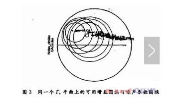
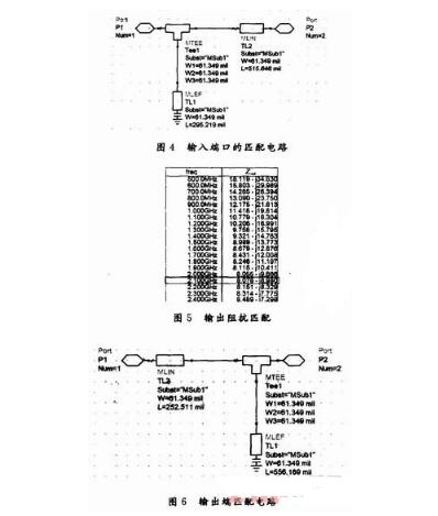
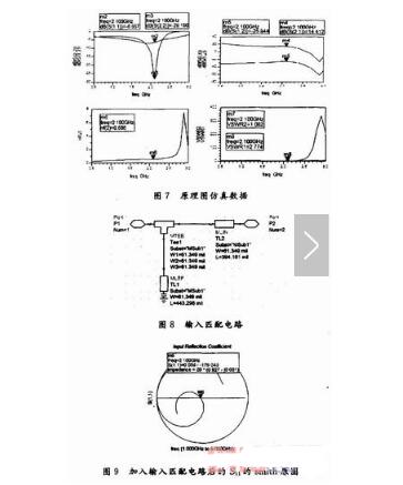
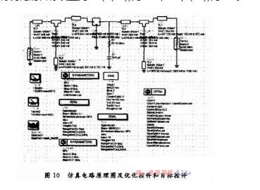
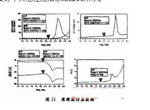
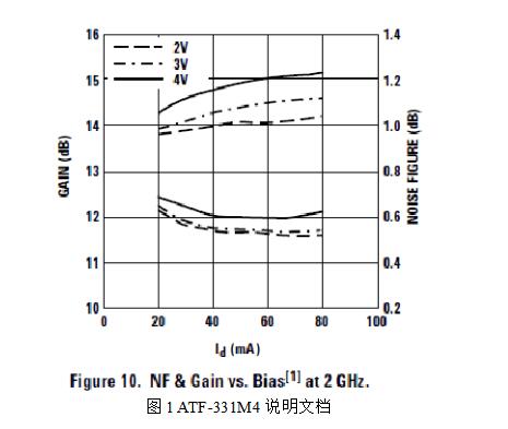
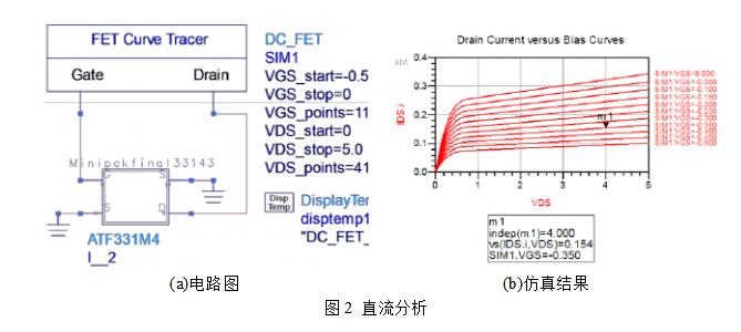
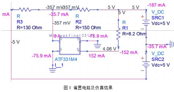
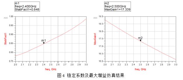
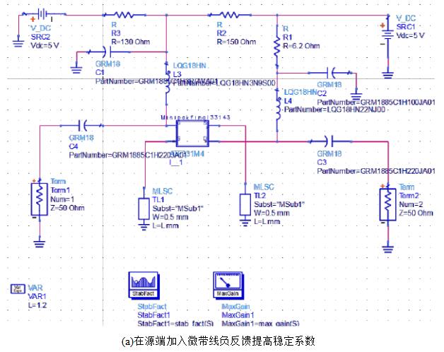
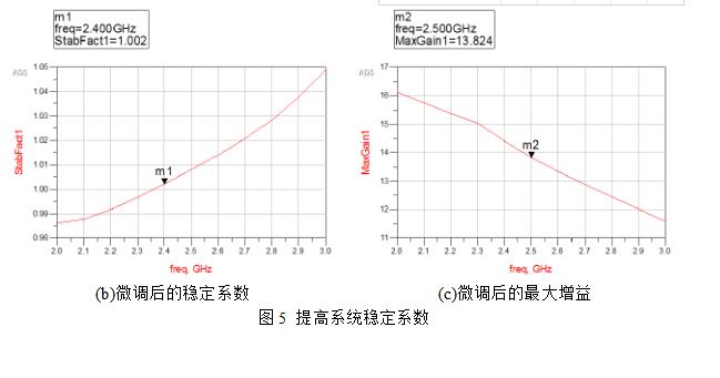
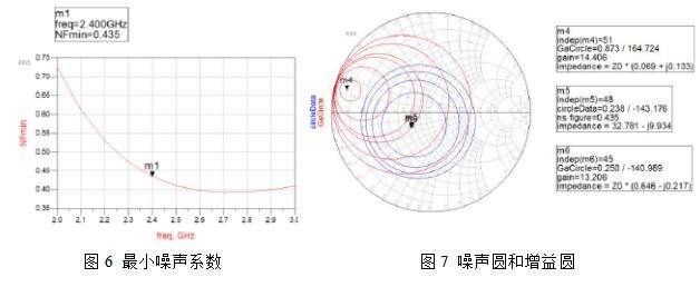
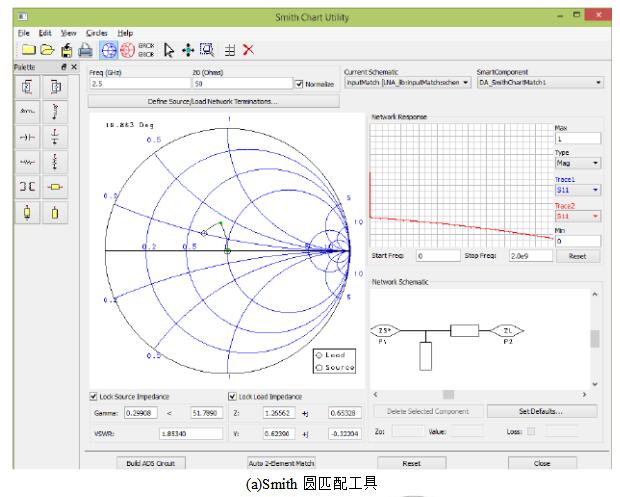
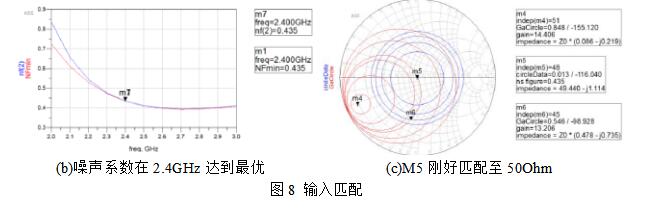
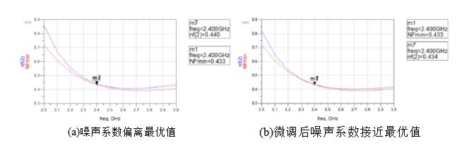
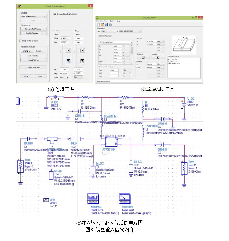
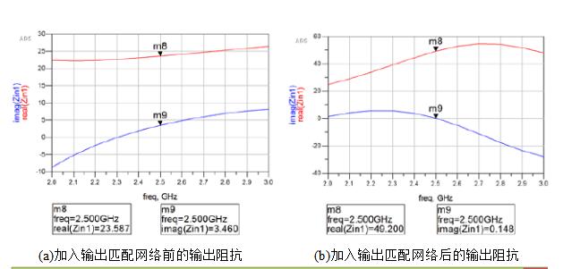
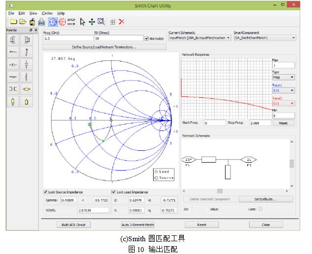
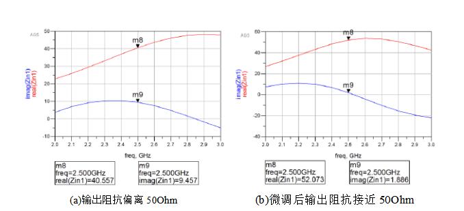
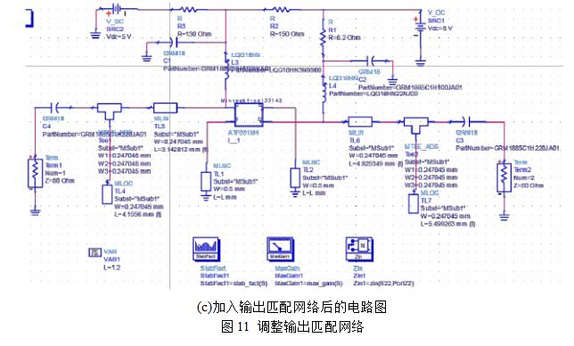
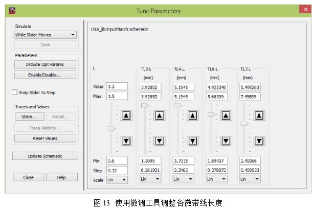
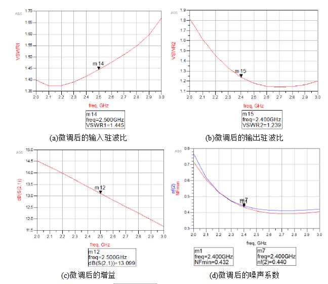
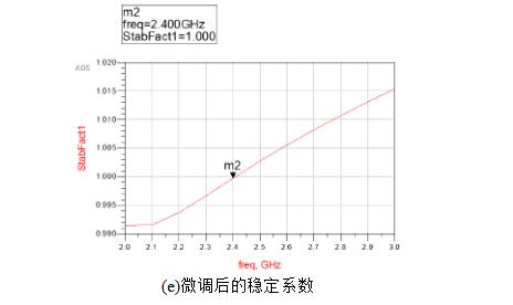
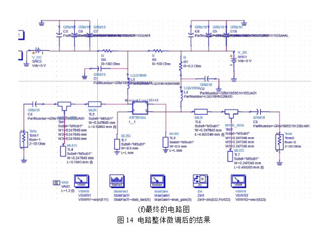
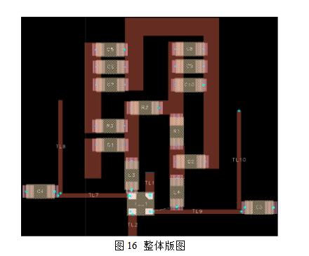
The low noise amplifier (LNA) is an important component of the RF transceiver, which can effectively improve the receiver's receiving sensitivity and thus increase the transmission distance of the transceiver. Therefore, the design of the low noise amplifier is good, which is related to the communication quality of the entire communication system. In this paper, the transistor ATF-54143 is taken as an example to illustrate the design method of two different low noise amplifiers, the frequency range is 2~2.2 GHz; the transistor operating voltage is 3 V; the operating current is 40 mA; the input and output impedance is 50 Ω. . 1.1. Modeling of Transistors Through the network, you can consult the relevant information of the transistor manufacturer. You can download the transistor model provided by the manufacturer, or you can download the S2P file of the tube according to actual needs. In this example, the S2P file of the tube is directly imported into the software, and the S parameter is used as a model design circuit. If it is the first import, you can use the module S-Params for S-parameter simulation to observe whether the obtained S-parameter is the same as the data provided by the S2P file. At the same time, measure the input impedance of the transistor and the corresponding minimum noise figure, and determine the transistor. Stability, etc., to prepare for the next step. 1.2, transistor stability After the S-parameter simulation of the circuit is completed, it can be obtained that the mu of the input/output terminal is less than 1 at a frequency of 2 to 2.2 GHz, and the transistor is unstable according to the radio frequency correlation theory. By connecting a 10 Ω and 5 pF capacitor in parallel with the output, the values ​​of m2 and m3 are both greater than 1, as shown in Figure 1, Figure 2. The transistor achieves stable conditions within the bandwidth and measures an input impedance of 16.827-j16.041 at 2.1 GHz. At the same time, it was found that Fmin increased from 0.48 to 0.573 due to the addition of a resistor at the output, Γopt was 0.329∠125.99°, Zopt=(30.007+j17.754)Ω. Among them, Γopt is the best source reflection coefficient. 1.3, develop a plan As shown in FIG. 3, the available gain circle family and the noise figure circle family are drawn on the same Γs plane. According to the analysis, if the available gain circle passes the position of the point where the optimal noise figure is located, and the input circuit is matched according to the point, the noise figure is the smallest for the LNA, but the gain does not reach the maximum. Good amplification. So it is traded in by sacrificing the available gain. In this case, the transistor gain can reach about 14 dB and Fmin is about 0.48, as shown in Figure 3. Another solution is to strike a balance between the available gain and the noise figure, with the goal of using small noise matching as much as possible, using a design that balances gain. In this case, the transistor gain is about 15 dB and Fmin is about 0.7 (see Figure 3). This is the second option mentioned in this article. 2.1, input matching circuit design For the low noise amplifier, in order to obtain the minimum noise figure, Γs has an optimal Γopt coefficient value, and the LNA reaches the minimum noise figure, that is, the optimal noise matching state is achieved. When the matching state deviates from the optimal position, the noise figure of the LNA will increase.å‰é¢opt=0.329∠125.99° has been obtained in the previous qualitative analysis, and the corresponding Zopt=30.007+j17.754 Ω. The ADS Passive Circuit/Micorstrip ControlWindow tool can be used to automatically generate matching circuits for input ports. Add a DA_SSMatehl smart module to the schematic and modify the settings: F=2.1 GHz, Zin=50 Ω. It is worth noting that when using this tool to generate matching circuits, Zload is the conjugate of Zopt. After setting, add a MSub control, which is mainly used to describe the basic information of the substrate. Modify the settings to H=0.8 mm, Er=4.3, Mur=1, Cond=5.88× 10⁷, Hu = 1.0e + 33 mm, T = 0.03 mil. After the setting is completed, the automatic matching circuit can be generated, and the result circuit is as shown in FIG. 4. Add the input matching circuit to Figure 1 and then simulate the S parameters. It can be seen that the position of the optimum noise figure Γopt is successfully matched to the 50 Ω position due to the addition of the input matching circuit. 2.2, output matching circuit design According to the principle of maximum power gain, the design of the output matching circuit is carried out (taking into account the existence of the output stabilization circuit and the influence on the output impedance, the stability circuit should be included in the measurement of the output impedance), that is, the output impedance (Zopt=8. 055-j8.980, as shown in Figure 5) is matched to 50 Ω using the method described above. The resulting output matching circuit is shown in Figure 6. 2.3, simulation results Observing the final simulation results, we can see that the gain is 14.4 dB; the noise figure is 0.586, which is very close to the optimal noise figure of the stable transistor of 0.573, and the gain flatness is low and the stability is excellent. The specific performance indicators are shown in Figure 7. 3.1, input matching circuit design If the substrate material is selected to be a glass epoxy FR-4 substrate with a dielectric constant of 4.3 and a thickness of 0.8 mm, the transistor input impedance at 2.1 GHz is 16.827-j16.041. Using the above matching circuit generation method, the input matching circuit is designed using a single-branch module in the ADS design wizard. The matching circuit in Figure 8 can be obtained very quickly. As shown in Fig. 9, m6 = 50 (0.927 + j0.001) in the figure. Very close to 50 Ω, so the resulting input matching is reasonable. 3.2, output matching circuit design After the input matching circuit design is completed, the output matching circuit can be designed. Here, the advantages of CAD software are fully utilized and realized by means of optimization. The basic process is as follows: Add the result of the input matching circuit to Figure 10 and add the microstrip as shown at the transistor output. Bring up the optimization control and set the optimization target to -20 for dB(S(11)) and -15 for dB(S(22)). At the beginning of the optimization, the width of TL1, TL2, and TL3 is set to 61.394 mil, which is to ensure that the characteristic impedance of the microstrip line is 50 Ω considering the factors such as the thickness of the sheet and the sheet. Preset the length of TL1, TL2, TL3. After optimizing once, refresh the result, observe whether the indicators of various charts are better, whether the value reaches the set maximum value, and if the maximum value is reached, change the set value again to re-optimize. After repeated iterations, it will be able to change these values ​​again. If the change is not effective for various indicators, you can try to change the resistance and input matching values ​​and optimize. Through repeated debugging, it is found that R1 is set to 15 Ω, and after adding TL7, the gain and noise figure and the input-output standing wave ratio effect are better. The schematic diagram of the simulation circuit and the optimization control and target control are shown in Figure 10. 3.3, simulation results Observing the final simulation results, we can see that the gain is 15.816 dB and the noise figure is 0.708. This index is better than the qualitative analysis. Other performance indicators are shown in Figure 11. Low noise amplifier design steps 1. DC analysis and bias circuit design 2, stability analysis 3, the noise circle coefficient matches the input 4, the maximum gain output matching 5, the overall fine-tuning of the circuit 6, layout design 1. As can be seen from the description of ATF-331M4, at 2GHz, the noise figure is about 0.6 when VDS is 4V, Id is 40-80mA, and the gain is above 15dB, which meets the design requirements. In order to make the gain as large as possible, determine the bias of the transistor VDS=4V, Id=80mA; 2. Download the model of ATF-331M4 from Avago's official website, and perform DC analysis under ADS2015.01 as shown in Figure 2. Bias the voltage of VGS. Since the ATF-331M4 has two sources, in order to make the current of each source terminal 80mA, the gate voltage of Id is about 160mA. From the DC simulation results, the VGS is about -0.35V; 3. After determining the static working point, the bias circuit can be designed. Originally, there is a "DA_FETBias" control tool in ADS that can easily design a bias circuit. However, since the gate voltage of the transistor needs to be biased to a negative voltage, this tool is difficult to perform, so the bias circuit can only be manually designed. Using a dual supply of +5V and -5V and a nominal resistance value, the gate voltage of the voltage divider is approximately -0.35V when the two resistors are 130Ohm and 150Ohm, respectively. Since the drain current is about 160 mA, the drain resistance can be calculated to be about 6.2 Ohm when the drain voltage is 4V. Finally, the circuit diagram and DC simulation results are shown in Figure 3. 1. Add 3.9nH choke inductors L1 and L2, 3.9pF bypass capacitors C1, C2 and 22nH DC blocking capacitors C3 and C4 to the circuit diagram, then add 50Ohm Term control and StabFact at the input and output terminals. And the MaxGain control for S-factor simulation. As shown in Fig. 4, the stability coefficient K is 0.848 at 2.4 GHz, the circuit is unstable, and the circuit has a MaxGain of 17 dB at 2.5 GHz. 2. In order to stabilize the system, a microstrip line is added at the source end as the inductor to introduce negative feedback as shown in Fig. 5a. At the same time, use the variable control to adjust the length of the microstrip line and repeat the simulation. Finally, when the length is 1.2 mm, the stability coefficient K is 1.002 at 2.4 GHz, and the system is stable, but MaxGain is reduced to 13.8 dB. 1. Perform noise simulation and draw NFmin parameters. As shown in Figure 6, NFmin is 0.435dB at 2.4GHz. The next step is to design an appropriate output matching network to achieve the minimum noise figure; 2. Draw a noise circle and a gain circle as shown in Figure 7. Where M4 is the input impedance with the largest gain, the gain is 14.406; M5 is the input impedance with the least noise, and the minimum noise figure is 0.435dB. But the two do not overlap and need to be balanced between the two. For low noise amplifiers, especially first stage amplifiers, the primary consideration is minimum noise. Therefore, the impedance of the M5 point, that is, 32.781-j9.934 is selected as the impedance of the input terminal for matching. At this time, the gain is about 13.206dB, which still meets the design requirements; 3. As shown in Figure 8, the Smith circle matching tool DA_SmithChartMatch is used for input impedance matching to generate a matching network using the microstrip line. Simulation again, it can be seen that the M5 point of the noise circle is exactly matched to 50Ohm, and the noise figure nf(2) is equal to NFmin at 2.4GHz, that is, the noise figure has been optimized; 4. As shown in Figure 9, the generated matching network is placed in the circuit diagram and moved to the DC blocking capacitor. Then, the LineCalc program is used to convert the microstrip line to the actual length and then simulate. It can be seen that the noise optimization point has deviated from 50 Ohm at this time, and the noise figure nf(2) deviates from the minimum noise figure NFmin. Therefore, the fine-tuning tool is used to fine-tune the microstrip line length of the input matching network to optimize the noise figure. 1, using the Zin control to measure the output impedance as shown in Figure 10a is 23.587 + j3.46 Ohm, that is, the output impedance matching needs to match 50Ohm; 2. Figure 10c uses the Smith circle matching tool DA_SmithChartMatch for output impedance matching to generate a matching network using microstrip lines. Simulation again, Figure 10b shows that the output impedance is very close to 50 Ohm; 3. As shown in Figure 11, the generated matching network is placed in the circuit diagram and moved to the DC blocking capacitor, and then the line is converted to the actual length using LineCalc and then simulated. This input output impedance has deviated from 50 Ohm. Therefore, the fine-tuning tool is used to fine-tune the microstrip line length of the output matching network, and the output impedance is close to 50 Ohm. 1. Simulate the circuit by adding 1uF, 0.01uF and 10pF three decoupling capacitors from the power supply at the positive and negative power supply. Figure 12 shows that the input standing wave ratio VSWR (input) is 1.832, greater than 1.5 design requirements, while the actual gain of S21 is 12.833dB, less than the required 13dB; 2. The method of fine-tuning the circuit is as follows: (1) Gain and absolute stability coefficient K value adjustment: Mainly adjust the source negative feedback microstrip lines TL1 and TL2. The gain and the absolute stability factor are a pair of contradictions. When the negative feedback is adjusted, the gain rise will inevitably lead to a decrease in the absolute stability coefficient K value. Therefore, the gain and the absolute stability factor K make a compromise. But the stability of the circuit system must be guaranteed, ie K"1. Adjusting the input-output standing wave ratio VSWR also has some effect on the gain; (2) Input VSWR (input) adjustment: Mainly adjust the input matching circuit microstrip lines TL3 and TL4. To reduce VSWR (input), adjust the impedance of the input to 50 Ohm when adjusting TL3 and TL4, so that the input reflection coefficient is minimized, thus reducing the input standing wave ratio VSWR (input). However, the adjustment of the input network will affect the noise figure and gain; (3) Adjustment of output standing wave ratio VSWR (output): Mainly adjust the output matching circuit microstrip lines TL6 and TL7. In order to reduce the VSWR (output), the impedance of the output should be adjusted to 50 Ohm to minimize the reflection coefficient at the output, thereby reducing the output standing wave ratio VSWR(output); (4) The input VSWR (input) and the output standing wave ratio VSWR (output) adjustment will affect each other; 3. The simulation results obtained after fine-tuning the length of each microstrip line as shown in Fig. 13 are as follows. Figure 14 shows that the VSWR (input) is 1.445 and the VSWR (output) is 1.239, both of which are less than 1.5. The S21 representing the actual gain is 13.0399, the noise figure nf(2) is 0.44, and the stability coefficient at 2.4 GHz is 1.0. The system is stable. Each parameter meets the design requirements. 1. Since the ATF-331M4 model does not have a layout, it needs to be drawn by itself. According to the size data in the specification, the layout of the drawn transistor is as shown in FIG. 15; 2. Manually layout and route all components after importing them into the layout. The smaller the distance between the discrete components, the better. Finally, the layout is shown in Figure 16. Stainless Steel Capillary Pipe Stainless Steel Capillary Pipe, Stainless Steel Capillary Tube, Stainless Steel Capillary Tubes With Hole, SS Capillary Tubes ShenZhen Haofa Metal Precision Parts Technology Co., Ltd. , https://www.haofametals.com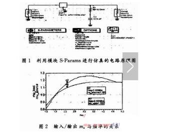


Two Design Methods for Low Noise Amplifiers and Low Noise Amplifier Design Examples
Two design methods for low noise amplifiers