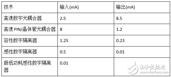
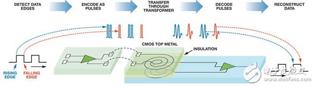
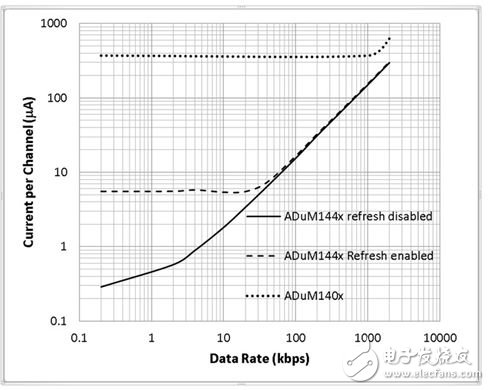
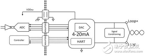
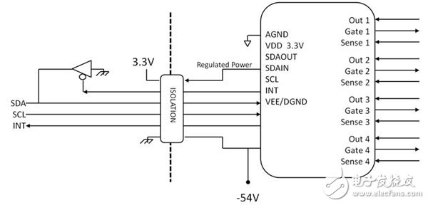
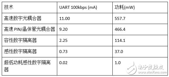
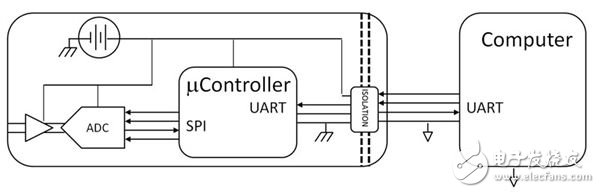
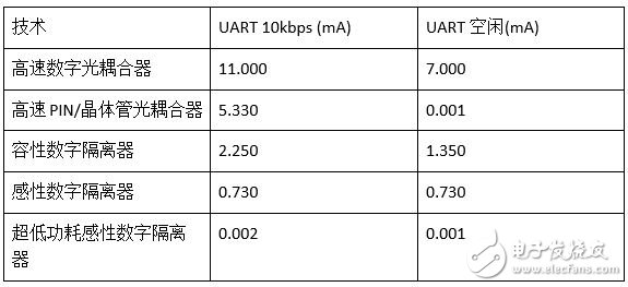
In the eyes of designers, isolation is an indispensable burden. Segregation is essential because it ensures the safety of electronic devices and is made available to anyone. Isolation is a burden because it limits communication speed, consumes a lot of power, and takes up board space. Optocouplers based on old technology, and even many newer digital isolators, consume a lot of energy, and as a result, some types of applications lose their practical value. In this article, we will examine the latest developments in ultra-low power isolation technology and its relationship and implementation with existing technologies. We will also explore several applications that can benefit from these new devices. For designers, the emergence of modern optocouplers about 45 years ago is a huge leap. With them, feedback can be implemented in the power control circuit, signal isolation in the communication circuit to disconnect the ground loop, and communication to the high-end power transistor or current monitor can be achieved. In the 1970s, a large number of optoelectronic devices emerged. These devices have affected the development of communication standards such as RS232, RS485 and industrial buses such as 4~20mA current loops, DeviceNet and Profibus. Affected by the limitations of the isolation device itself, the optical isolation function determines the many characteristics of these communication buses. In the next 20 years, the development of isolation technology is basically a quantitative change, and by 2000, the first batch of new chip-scale digital isolators appeared on the market. These new devices have used inductive coupling technology, chip-scale transformers, GMR materials, and later differential capacitive coupling techniques. These new technologies can support much higher speeds and much lower power levels than older optocouplers, but many of the new devices' features, such as high rates, are underutilized in the context of established standards. Because the existing standard interface does not have this requirement. The encoding and decoding electronics in digital isolators are made in standard packages and IC processes, making the addition of digital functions simple and easy. Low power consumption, low supply voltage support, and high integration have become major design advantages of non-optical couplers. Innovations that enable isolation to achieve higher speeds and lower power consumption will support the most demanding new interface standards. Currently, the power consumption of digital isolators is significantly lower than that of optocouplers, but it needs to be two to three orders of magnitude lower to enter new applications. So far, high performance isolation has not achieved this goal. The performance improvement of the isolation device is the result of the interaction between the data encoding scheme and the data transmission medium efficiency. In this article, we will focus on various aspects of determining power consumption. The encoding and decoding scheme can be roughly divided into two systems based on edge-encoded pulses and level-encoding systems. The simplest level system must continuously push energy through the isolation barrier to maintain a high level output state and a low level output state when no energy is being sent to the isolation barrier. In an optical coupler, energy transfer is facilitated by light, which is inefficient compared to the direct formation of an electric or magnetic field, and the detection efficiency of the receiving element end is also unsatisfactory. Therefore, an optical coupler based on a simple transistor or a PIN diode consumes a large amount of energy to generate light to keep the output on, but the receiver receives only a small amount of energy. This situation is shown in Table 1, which shows the power consumption of the PIN diode receiver optocoupler. On average, high input current and low output current are characteristics of such optocouplers. Table 1: Comparison of power consumption per channel of the isolator (VDD = 3.3V, 100kpbs) By adding active amplification to the receiver, the faster digital optocoupler reduces the amount of light needed to maintain a certain state. Although this method reduces the average current demand of the LED, the quiescent current of the receiver is relatively large, so the power consumption is not really reduced, but only transferred to the receiver. Reducing the required power consumption requires an increase in the efficiency of the LED and receiver components, or a change in the coding scheme. This is why optocoupler technology has not made a breakthrough in such a long period of time. In many capacitively coupled digital isolators, the system is actually similar to an optocoupler. This type of device uses a high frequency oscillator to send a signal through a pair of differential capacitors. Just like the optocoupler's LED, the oscillator needs to consume power to send a high state and turn off to send a low state. The receiver is equipped with an active amplifier that consumes bias current in both states. As shown in Table 1, the total power consumption is significantly lower than the optocoupler scheme due to the high coupling efficiency of the capacitor. It should be noted that the power level of the digital isolator is roughly equivalent, whether it is an inductive coupling or a capacitive coupling scheme. In this case, the main decision on the lowest power level is the coding scheme, especially at low data rate conditions. Analog Devices' iCoupler-based digital isolators (such as the ADuM140x family) use another encoding scheme, as shown in Figure 1. This scheme detects the edge at the input and encodes it as a pulse. For the ADuM140x, one pulse represents the falling edge and two pulses represent the rising edge. These pulses are coupled to the secondary side by a small transformer within the chip. The receiver counts the pulses and reconstructs the data stream. The pulse itself is very robust and has a good signal-to-noise ratio, but its width is only 1 ns, so the energy per unit pulse is low. This creates an excellent property: when there is no data change, the state is stored in a latch at the output, consuming almost no power. This means that power consumption is the sum of the integrated power in the pulse stream and some bias current. As the data rate decreases, power consumption decreases linearly and continues to DC. Similarly, the implementation of power consumption degradation is the coding scheme rather than the specific data transmission medium, which can be either a capacitive system or an optical system. Figure 1: Graphical illustration of a pulse coding scheme for a digital isolator. Detect data edges: Detect data edges Encode as pulses: coded as a pulse Transfer through transformer: via transformer coupling Decode pulses: Decode pulses Reconstruct data: Refactoring data Rising edge: rising edge Falling edge: Falling edge CMOS top metal: CMOS top metal Insulation: isolation The pulse coding scheme is not a panacea for low power consumption. The disadvantage is that if there is no logical change at the input, no data is sent to the output. This means that if there is a different DC level at the input and output during the power-up sequence, the input and output will not match. The ADuM140x solves this problem by setting a refresh watchdog timer on the input channel. If no activity is detected for more than 1μs, the timer will resend the DC state. The result of this design is that this encoding scheme will not continue to reduce power consumption when the data rate is below 1 Mbps. In fact, the device always runs at a data rate of at least 1 Mbps, so at low data rates, power consumption does not continue to drop. Even so, the average power consumption of the pulse coding scheme is lower than that of the level-sensitive scheme, as shown in Table 1. The ADuM140x pulse coding scheme was originally optimized for high data rates and is not intended to achieve the absolute lowest power consumption. This coding scheme has great potential for further power reduction, especially in the DC to 1 Mbps frequency range. This range of data is the range used by a large number of isolated applications, especially those with low power requirements. The four-channel ADuM144x and dual-channel ADuM124x series based on iCoupler technology use the following innovations. 1. Designed in a low voltage CMOS process 2. Evaluate all bias circuits and minimize or eliminate bias. 3. The frequency of the refresh circuit is reduced from 1MHz to 17KHz. 4. The refresh circuit can be completely disabled to achieve the lowest power consumption The power consumption is a function of frequency, as shown in Figure 2, and its reference object is ADuM140x. With refresh enabled, for the ADuM140x, when the data rate is 1Mbps, the curve inflection point caused by the refresh is clearly visible, and the ADuM144x is clearly visible at a data rate of 17kbps. At 1 kbps, the typical power consumption of each channel of the ADuM144x is 65 times lower, and when the refresh is completely disabled, it is about 1000 times lower. Figure 2: Total power consumption per channel for ADuM144x and ADuM140x devices at VDDX = 3.3V. Current per Channel (μA): current per channel / μA Why is the sharp drop in power consumption useful? In the following three applications, conventional optocouplers and digital isolators have limited or no utility at all. 4mA to 20mA isolated loop-powered field instrument The power budget of a loop-powered field instrument (see Figure 3) is very limited because all power comes from a 4 mA loop current. Fortunately, the loop typically provides enough voltage (typically 24V) to get approximately 100mW from the system. At 4 mA, the entire application will use a loop voltage of approximately 12V. Within this budget, a simple DC/DC converter can power the isolated sensor ADC and controller. Figure 3: Loop-powered field instrumentation. Controller: Controller Isolation: isolation Signal conditioning: signal conditioning Loop+: Loop + Loop-: Loop - Even assuming a high efficiency of the DC-DC converter and a voltage step-down ratio of 2:1, a typical sensor front end can use less than 4 mA at 3.3 V, and the power budget at the loop end is roughly equivalent. The main interface is the SPI bus that connects to the ADC. Each end of the isolated interface, as well as all controller ADCs and signal conditioning components, is powered by a loop. Table 2 shows the power consumption of a 4-wire SPI bus for each isolation technique. SPI 1 is the isolated loop-side current and SPI 2 is the required sensor-side current. At each end of the isolated interface, the optocoupler consumes many times more power than the power budget. Table 2: Total Power Consumption on Each Side of a 100kbps Isolated SPI Interface Capacitive digital isolators consume the full power budget of the field instrument. One possibility is to choose the ADuM1401, but the rest of the system has a small power budget, even if it only supports a single SPI interface to the ADC. The new ultra-low-power digital isolator based on iCoupler technology, the ADuM1441, consumes very little power and is only a small fraction of the power budget. This technology not only allows the application to work within its power budget, but also allows the addition of a second four-channel isolator to support a HART modem interface and an intelligent front-end controller, as shown in the dotted line in the figure. The ultra-low power iCoupler technology enables new features that were previously not possible in isolated applications. Telecommunications applications such as Power over Ethernet (POE) derive power from a relatively high voltage supply rail that is powered by Ethernet. The control communication interface must draw power from an isolated DC/DC converter or take power from a -54V bus voltage through a regulator. In the example shown in Figure 4, the 3.3V communication interface voltage for the I2C control bus is generated by a regulator built into the POE controller. Table 3 shows the current required to run the I2C bus interface on the POE controller side, as well as the power consumed by the POE controller to support each technology. Figure 4: Power over Ethernet I2C communication bus. Isolation: isolation Regulated Power: Adjusted power supply Table 3: Total power consumption of isolation technology in POE applications The optocoupler solution produces half a watt of heat in the chip, and the chip is likely to be near its thermal limit. From top to bottom in the table, each interface performs slightly better than the previous one. Finally, the ADuM1441 with ultra-low power consumption consumes about 1mW. As a result, the thermal load of the interface is negligible in this chip. Even if the power supply is not regulated inside the POE chip, the power consumption is very low, and a simple Zener diode and resistor can be used to achieve a reasonable level of cost and cooling load for the energy-saving component. This technology simplifies the power architecture. The third use of ultra-low power is to support battery-powered applications that last for long periods of time. Medical devices for home health monitoring (such as blood glucose meters, pulse oximeters) must have a special structure to connect to a patient and connect to a non-medical computer (see Figure 5). The serial interface must be powered and can wake up the device when it is connected to the computer, so an active isolator should be used in the standby circuit. In this case, with the refresh disable feature of the ADuM1441, the device draws less than 4μA from the battery. For such a low power consumption level, even a button cell can keep the standby current for several years. Figure 5: Battery powered medical sensor solution. Computer: Computer In addition, thanks to the ultra-low power consumption of the ADuM1441, it is easy to power the computer-facing side of the isolation component. Since the interface requires only a few μA of current, a single state line can be used to power the isolator in the serial interface, thus eliminating the need for a dedicated power supply. Table 4 shows some of the properties of optocouplers and various digital isolation schemes in standby mode. Note that if the correct idle state is selected, the standby current of the PIN/transistor is actually as low as the iCoupler-based ultra-low power products. Many applications take advantage of this property of optocouplers to achieve ultra-low standby power consumption. However, once communication begins, power consumption jumps to a relatively high level, which is not the case with the ADum1441 solution. Table 4: Low speed and idle total power consumption of the isolator 2-in-1 Tablet, tablet with keyboard, android tablet with case tablet with pen, mini laptop C&Q Technology (Guangzhou) Co.,Ltd. , https://www.gzcqteq.com