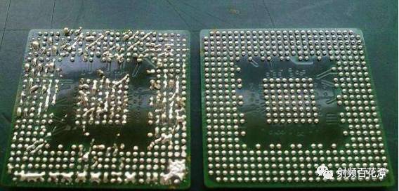
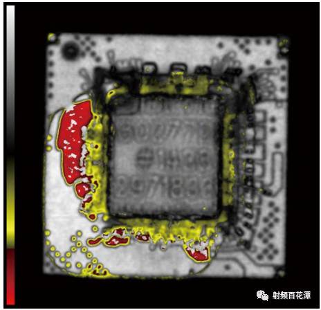
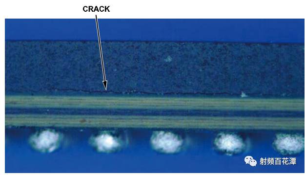
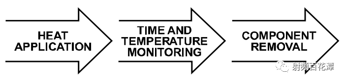
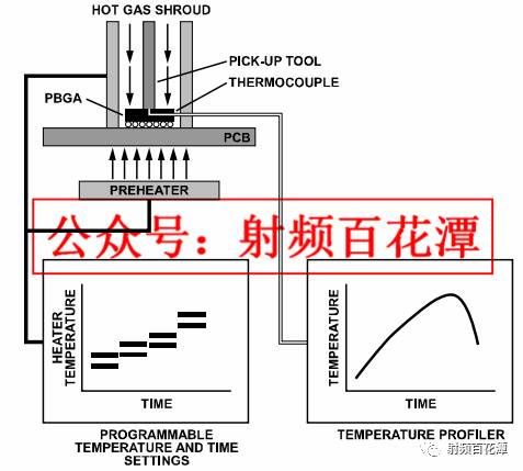
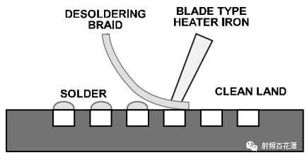
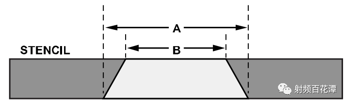
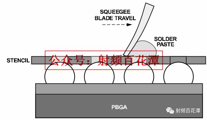
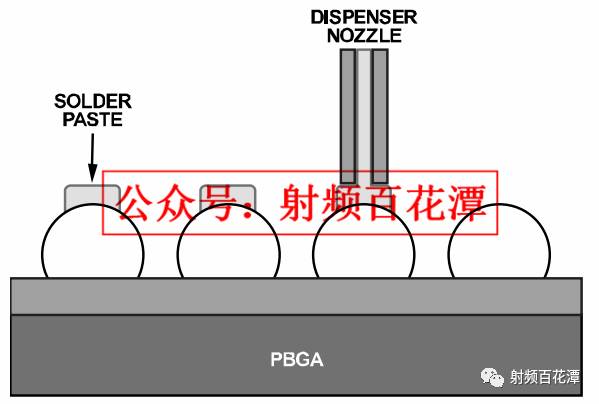
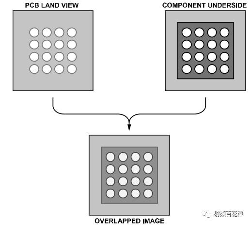
Introduction This application note describes the recommended procedure for removing a molded ball grid array package (PBGA) from a printed circuit board (PCB). If you make such a mood, it will be very bad~~ Package description PBGA is a package form whose main distinguishing feature is the use of a solder ball array to contact a substrate such as a PCB. This feature gives the PBGA an advantage over other pin configurations (eg single-row, dual-in-line, quad-array), which is the ability to achieve higher pin densities. The interconnection inside the PBGA package is achieved by wire bonding or flip chip technology. The PBGA chip including the integrated circuit is packaged in a molding material. Figure 1. Schematic of the PBGA device PBGA device repair After the PBGA device is assembled on the PCB, if a defect is found, it should be repaired to remove the defective device and replaced with a working device. Before removing the device, the defective device should be heated until the solder joint is liquefied to remove the bad device from the board. The general rework procedure is as follows: 1. Prepare the board. 2. Remove the device. 3. Clean the PCB pads. 4. Apply solder paste. 5. Device alignment and placement. 6. Fix the device. 7. Check. Remove device and layer Mechanical stress may be generated on the PBGA and/or PCB when the device is removed. Care should be taken to remove defective components from damage to the PCB, adjacent devices, and defective devices themselves, especially if the user intends to troubleshoot a defective device. Excessive stress on PBGA devices, such as heating the device above the rated peak temperature or overexposure to high temperatures, can result in package delamination or external physical damage (see Figures 2 and 3). For devices that require further analysis, delamination caused by improper removal increases the difficulty of finding the true failure mechanism. Therefore, in order to carry out effective fault analysis, it is necessary to properly remove bad devices. Figure 2. Overheating causes delamination between the substrate and the molding material of the PBGA device (observed by scanning acoustic microscope) Figure 3. Low magnification image of overheating causing cracks on the PBGA (side view) Prepare the board It is highly recommended to dry the PCB components before the start of the repair to eliminate residual moisture. If not eliminated, residual moisture may damage the device due to the "popcorn effect" during reflow. Bake the PCB assembly at 125 ° C for at least 4 hours as long as these conditions do not exceed the rating limits of other devices on the PCB. If these conditions exceed the rating limits of other devices, the alternative baking conditions described in the joint industry standard IPC/JEDEC J-STD-033 should be used. Remove device Different tools can be used to remove the device. To remove the device, it may be necessary to heat the device until the solder reflows and then mechanically remove the device while the solder is still in a liquid state. A programmable hot air rework system provides controlled temperature and time settings. The temperature profile used for the assembly of the device should be followed for repair. The rework temperature must not exceed the peak temperature specified on the Humidity Sensitivity Level (MSL) label. The heating time can be shortened (for example, for the liquefaction zone) as long as the solder is completely reflowed. The solder reflow zone should be at peak temperature for less than 60 seconds. The vacuum pressure of the pick-up tool should be less than 0.5 kg/cm2 to prevent the device from ejecting before reaching full reflow and to avoid pad floating. Do not use devices removed from the PCB. Control the rework temperature to avoid damage to the PBGA device and PCB. Consideration should be given to PBGA heating rates may be faster due to differences in thermal mass compared to lead frame based packages such as standard outline integrated circuits (SOIC) and lead frame chip scale packages (LFCSP). Note that covering the area around the device with a heat-resistant tape provides further protection. In addition, it is recommended to heat the underside of the PCB to reduce the temperature difference between the upper and lower sides of the PCB to minimize plate bending. The temperature profile should be calibrated when defining the rework tool settings. This calibration is especially important when rewriting a particular device for the first time. PBGA devices also need to be calibrated with different body sizes, solder compositions or different PCB materials, configurations, sizes and thicknesses as they may have different thermal mass values. Calibration must include monitoring temperature, time, and other settings of the equipment tool (see Figure 4). Thermocouples should be assembled to different parts of the board assembly, such as the upper part of the PBGA device and the top of the PCB (see Figure 5). Analyze time and temperature profile data and obtain valid parameters for device removal from the evaluation. Figure 4. Simplified flow chart for device removal evaluation Figure 5. Schematic diagram of device removal calibration settings Cleaning the PCB pads After removing the PBGA device, the pads on the PCB will have too much solder and must be cleaned before the replacement PBGA device is installed. Pad cleaning can be divided into two steps: 1. Go to tin. Use solder wire and blade soldering iron to remove excess solder from the pads (see Figure 6). The width of the selected blade should match the maximum width occupied by the device. The blade temperature must be low enough to avoid damaging the board. Solder can be applied to the pad, and then the solder can be removed with a solder wire and a soldering iron. Figure 6. PCB pad de-tin 2. Clean. Clean with a cleaning agent on the return area and wipe clean with a lint-free cloth. The cleaning agent used depends on the type of solder paste used in the original assembly. Coating solder paste Solder paste should be applied before the replacement PBGA device is mounted on the board in order to replace the solder paste applied when the board is initially assembled, thus ensuring the reliability of the PBGA solder joint. The amount of solder paste applied to each solder ball must be the same to avoid non-coplanar problems when installing PBGA on the board. A template can be used to apply solder paste to the PCB pads. Template alignment accuracy is the key to maintaining reflow soldering uniformity. Use the same PBGA aperture geometry and stencil thickness as the board assembly. Use a trapezoidal aperture (see Figure 7) to ensure even solder paste release and reduce stains. Figure 7. Template aperture geometry (A longer than B) In some cases, it may not be possible to apply solder paste evenly and accurately to the PCB pads using a stencil, especially for boards with high device density or tight geometric space. In this case, solder paste should be considered applied to the solder balls on the bottom of the device. To this end, a solder paste can be applied to the upper end of the solder ball using a template, or solder paste can be dispensed to all solder balls (see Figures 8 and 9). Specially designed fixtures and/or rework equipment can be used to achieve this. Figure 8. Solder paste template to print solder paste onto solder balls Figure 9. Distributing solder paste onto the solder balls Device alignment and placement It is important to accurately place the device on the board. A placement device with a split-beam optical system facilitates alignment of the PBGA and the board. This type of imaging system involves overlaying a PBGA solder ball mirror image onto a PCB land image (see Figure 10). The placement machine must have the ability to support fine-tuning (including rotation) along the x-axis and y-axis. Figure 10. Aligning PCBs and devices with a split-beam optical system The placement accuracy depends on the equipment or process used. Although the PBGA package tends to be automatically aligned during reflow soldering, it should be ensured that the patch deviation is less than 50% of the PCB pad width. If the alignment error is too large, solder bridging may cause an electrical short. Fixed device Since all reflow parameters are optimized, the thermal profile established during the original assembly process should be used. an examination After reflow, inspect the assembled PBGA for defects such as misalignment or damage. Use X-ray inspection for problems such as solder bridging and solder balls. Perform an electrical verification test to verify that the device is functioning properly, if necessary. These machines are used for the production of nails ROYAL RANGE INTERNATIONAL TRADING CO., LTD , https://www.royalrangelgs.com