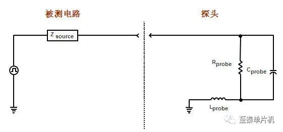
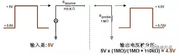
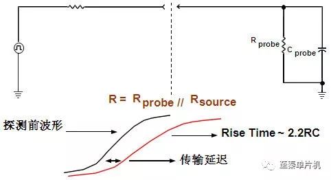
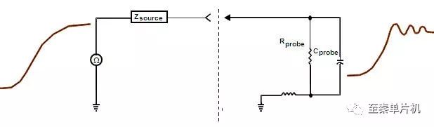
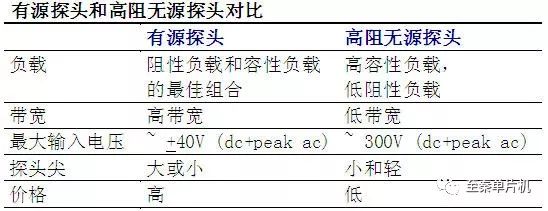
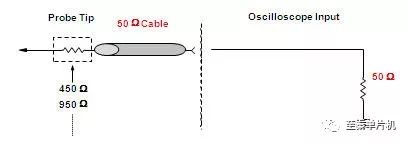
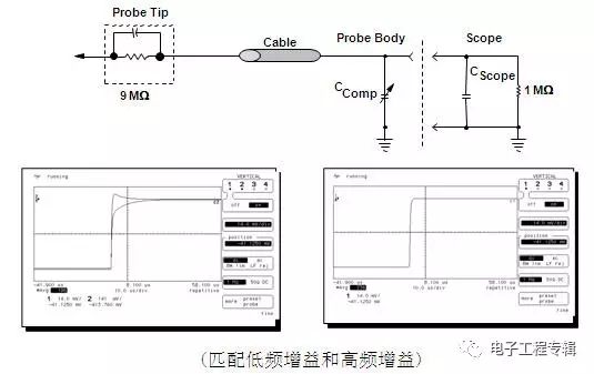
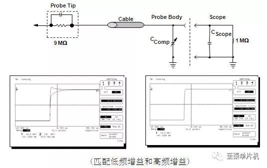
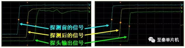
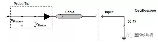
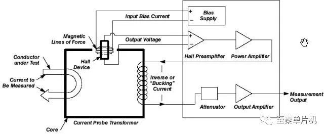
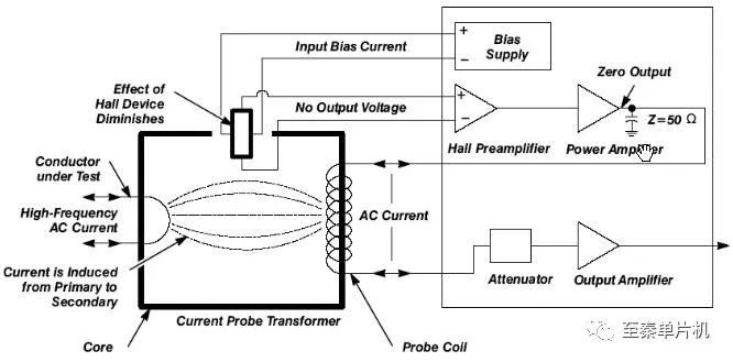
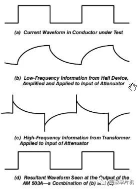
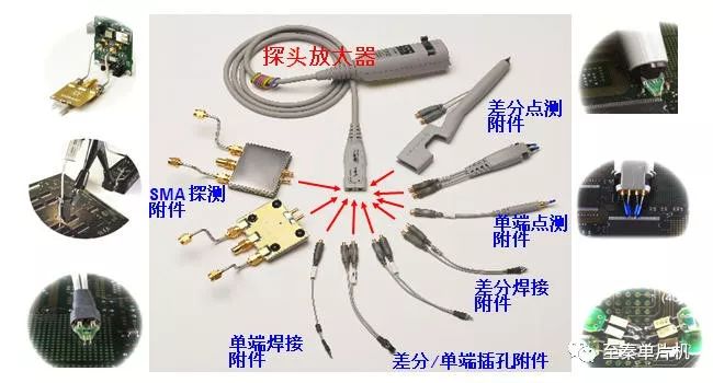
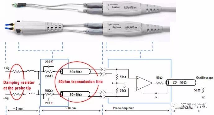
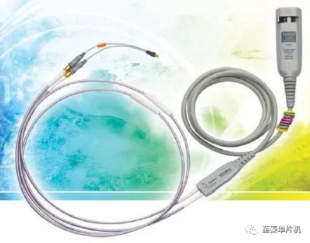
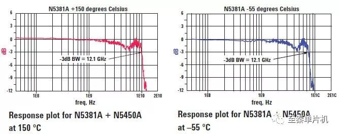
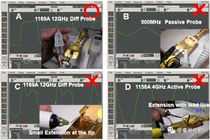
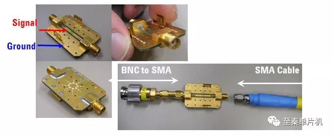
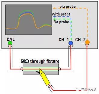
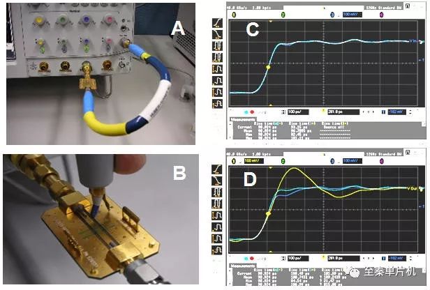
The oscilloscope extends the scope of the oscilloscope because of the presence of the probe, allowing the oscilloscope to test and analyze the electronic circuit under test online, as shown below: Figure 1 The role of the oscilloscope probe The choice and use of the probe need to consider the following two aspects: First, because the probe has a load effect, the probe will directly affect the signal under test and the circuit under test; Second: the probe is part of the entire oscilloscope measurement system Will directly affect the signal fidelity and test results of the instrument. First, the load effect of the probe When the probe detects the circuit under test, the probe becomes part of the circuit under test. The load effect of the probe includes the following three parts: 1. Resistive load effect; 2. Capacitive load effect; 3. Inductive load effect. Figure 2 Load effect of the probe The resistive load is equivalent to a resistor connected in parallel on the circuit under test, which has a voltage dividing effect on the signal under test, affecting the amplitude and DC offset of the signal under test. Sometimes, with the probe, the faulty circuit may become normal. It is generally recommended that the resistance of the probe R>10 times the measured source resistance to maintain an amplitude error of less than 10%. Figure 3 Resistive load of the probe The capacitive load is equivalent to a capacitor connected in parallel on the circuit under test, which has a filtering effect on the signal to be measured, affecting the rise and fall time of the signal under test, affecting the transmission delay and affecting the bandwidth of the transmission interconnection channel. Sometimes, with the probe, the faulty circuit becomes normal, and this capacitive effect plays a key role. It is generally recommended to use a probe with as small a capacitive load as possible to reduce the effect on the edge of the signal being measured. Figure 4 Capacitive load of the probe The inductive load is derived from the inductive effect of the probe ground, which resonates with the capacitive and resistive loads, causing ringing on the displayed signal. If there is a significant ringing on the displayed signal, check to see if it is the true characteristic of the signal being measured or the ringing caused by the grounding wire. The way to check is to use the shortest possible grounding wire. It is generally recommended to use the ground wire as short as possible. Generally, the ground wire inductance is 1nH/mm. Figure 5 Inductive load of the probe Second, the type of probes Oscilloscope probes can be divided into two major categories: passive probes and active probes. Passive power, as its name suggests, requires no power to the probe. The passive probe is subdivided as follows: 1. Low resistance resistor divider probe; 2. High impedance passive probe with compensation (the most commonly used passive probe); 3. High voltage probe The active probe is subdivided as follows: 1. Single-ended active probe; 2. Differential probe; 3. Current probe A simple comparison of the most commonly used high-impedance passive probes and active probes is as follows: Table 1 Comparison of active and passive probes The low-resistance resistor divider has a low capacitive load (<1pf), a high bandwidth (>1.5GHz), and a low price, but the resistive load is very large, typically only 500ohm or 1Kohm, so it is only suitable for testing low sources. Impedance circuit, or circuit that only focuses on time parameter testing. Figure 6 low input resistance probe structure High-impedance passive probes with compensation are the most commonly used passive probes. The probes that are standard on the general oscilloscope are all such probes. High-impedance passive probe with compensation has high input resistance (generally 1Mohm or more), adjustable compensation capacitor to match the input of the oscilloscope, high dynamic range, and can test large amplitude signals (tens of Above), the price is also lower. But I don't know where the input capacitance is too large (generally 10pf or more) and the bandwidth is low (generally less than 500MHz). Figure 7 Common passive probe structure The high-impedance passive probe with compensation has a compensation capacitor. When connecting the oscilloscope, it is generally necessary to adjust the capacitance value (you need to use the small screwdriver that comes with the probe to adjust, adjust the probe to the oscilloscope to compensate the output test position), Matches the oscilloscope input capacitance to eliminate low frequency or high frequency gain. On the left side of the figure below is the presence of high frequency or low frequency gain. The adjusted compensation signal display waveform is shown on the right side of the figure below. Figure 8 Compensation for passive probes The high-voltage probe is based on a passive probe with compensation, increasing the input resistance and increasing the attenuation (eg 100:1 or 1000:1, etc.). Because of the need to use high voltage components, high voltage probes are generally physically larger. Figure 9 Structure of the high voltage probe Third, the active probe Let us first observe the effect of testing a 1 ns rise time step signal with a 600 MHz passive probe and a 1.5 GHz active probe. Use a pulse generator to generate a 1 ns step signal. After passing the test fixture, connect directly to a 1.5 GHz oscilloscope using an SMA cable. This will display a waveform on the oscilloscope (blue signal as shown below). The waveform is saved as a reference waveform. Then use the probe test fixture to detect the signal under test. The waveform connected directly through the SMA becomes a yellow waveform due to the influence of the probe load, and the probe channel displays a green waveform. Then test the rise time separately, you can see the impact of passive probes and active probes on high-speed signals. Figure 10 Effect of passive and active probes on the measured signal and measurement results The specific test results are as follows: using 1165A: 600MHz passive probe, using the crocodile nozzle grounding wire: affected by the probe load, the rise time becomes: 1.9ns; the waveform displayed by the probe channel has ringing, and the rise time is: 1.85ns; Use 1156A: 1.5GHz active probe, use 5cm grounding wire: less affected by probe load, the rise time is still: 1ns; the waveform displayed by the probe channel is consistent with the original signal, and the rise time is still: 1ns. The structure of the single-ended active probe is as follows, using an amplifier to achieve impedance transformation. Single-ended active probes have a high input impedance (typically above 100Kohm) and a small input capacitance (typically less than 1pf). After connecting to the oscilloscope through the probe amplifier, the oscilloscope must use a 50ohm input impedance. The active probe has a wide bandwidth (now up to 30 GHz), but the load is small, but the price is relatively high (generally each probe reaches about 10% of the same bandwidth oscilloscope price), and the dynamic range is small (this needs attention, because the probe dynamics are exceeded) The range of signals can not be tested correctly. The general dynamic range is about 5V), which is relatively fragile and should be used with care. Figure 11 Active probe structure The differential probe structure is as follows, using a differential amplifier for impedance transformation purposes. Differential probes have a high input impedance (typically above 50Kohm) and a small input capacitance (typically less than 1pf). After connecting to the oscilloscope through a differential probe amplifier, the oscilloscope must use a 50ohm input impedance. The differential probe has a very wide bandwidth (now up to 30 GHz), a very small load, and a high common-mode rejection ratio, but at a relatively high price (generally about 10% of the oscilloscope price per probe) and a small dynamic range. (This needs to be noted, because the signal beyond the dynamic range of the probe can not be tested correctly. The general dynamic range is about 3V), it is relatively fragile, and care should be taken when using it. The differential probe is suitable for testing high-speed differential signals (no grounding during testing), suitable for amplifier testing, power testing, and applications such as virtual ground testing. Figure 12 Differential probe structure The current probe is also an active probe that uses a Hall sensor and an induction coil to measure DC and AC current. The current probe converts the current signal into a voltage signal, and the oscilloscope collects the voltage signal and displays it as a current signal. The current probe can test a current of several tens of milliamperes to several hundred amperes. When using it, it is necessary to draw a current line (the current probe is used to clamp the wire in the middle for testing without affecting the circuit under test). The working principle of the current probe when testing DC and low frequency AC: When the current clamp is closed and a current-carrying conductor is centered, a magnetic field will appear in response. These magnetic fields deflect the electrons in the Hall sensor and produce an electromotive force at the output of the Hall sensor. The current probe generates a reverse (compensated) current according to this electromotive force to the coil of the current probe, so that the magnetic field in the current clamp is zero to prevent saturation. The current probe measures the actual current value based on the reverse current. In this way, it is possible to measure large currents very linearly, including AC and DC mixed currents. Figure 13 How the current probe works when testing DC and low frequencies The working principle of the current probe when testing the high frequency: As the frequency of the measured current increases, the Hall effect gradually weakens. When measuring a high-frequency alternating current without DC component, most of it is directly induced by the strength of the magnetic field. To the coil of the current probe. At this point, the probe acts like a current transformer. The current probe directly measures the induced current, not the compensation current. The output of the amplifier provides a low-impedance ground loop for the coil. Figure 14 How the current probe works when testing high frequencies The working principle of the current probe in the intersection area: When the current probe works in the high and low frequency intersection area of ​​20KHz, part of the measurement is realized by the Hall sensor, and the other part is realized by the coil. Figure 15 How the current probe intersection area works Active probe accessories Modern high-bandwidth active probes are designed with a separate design, ie the probe amplifier is separated from the probe attachment. The benefits of this design are: 1, support more probe accessories, making detection more flexible; 2, protection investment, the most expensive is the probe amplifier (a probe amplifier can support a variety of detection methods, previously required several probes to achieve); at the same time probe attachment protection Probe amplifier (even if the probe accessory is damaged, the price is relatively cheap); 3, this design method is easy to achieve high bandwidth. Figure 16 Probe Accessories These probe accessories mainly include the following: 1, point probe accessories (including: single-end measurement and differential point measurement); 2, welding probe accessories (including: single-ended welding and differential welding, separate ZIF welding); 3, jack probe accessories; 4, differential SMA probe accessories (oscilloscopes generally support SMA connections directly, but if the signal under test needs to be pulled up like HDMI, the SMA probe accessory must be used). The circuit structure of the probe accessory is shown below: 1. There will be a pair of damping resistors (usually 82 ohms) at the tip end of the probe attachment. The effect of the damping resistor is to eliminate the resonance effect of the inductance of the tip end of the probe attachment; 2. Behind the tip of the probe is a 25Kohm resistor. This resistor determines the input impedance of the probe (DC input impedance is the resistance: single-ended 25Kohm, differential 50Kohm). This resistor makes the measured signal transmitted to the probe amplifier part very powerful. Small, does not have a greater impact on the signal under test. 3, 25Kohm resistor is followed by the coaxial transmission line part, this transmission line is responsible for transmitting small signals to the amplifier. The length of this transmission line can be very long or short, and an attenuator can be added in the middle, or a coupling capacitor can be added. 4. The coaxial transmission line is connected to the amplifier and the amplifier is 50 ohm matched (differential 100 ohm match). Figure 17 Structure of the active probe accessory In order to maintain the accuracy of the probe, the active probe needs to work at a constant temperature, so the probe amplifier cannot be placed in a high and low temperature chamber for testing the board under test in high and low temperature environments. It can be seen from the probe attachment structure that the length of the intermediate 50 ohm transmission line does not affect the detection, so it is possible to use a long coaxial cable or an extended coaxial cable to allow the coaxial cable to be inserted into a high and low temperature box for high and low temperature replacement. Board testing. The following figure shows the N5450A expansion cable, which can be operated from -55° to 150° using the N5381A soldering probe accessory. Figure 18 High and low temperature probe structure principle Using the N5450A expansion cable and the N5381A probe accessory, using the 1169A 12GHz probe amplifier, the frequency response curve in the -55° and 150° environments is shown in the figure below, which can be seen to meet the requirements of high-speed signal testing. Figure 19 Frequency response of high and low temperature probes at high and low temperatures V. Probe and accessory accuracy verification The following figure is an example: the signal to be measured is a clock signal with a frequency of 456MHz and an edge time of about 65ps. The test results of different types of probes and probe accessories are used respectively. Figure A shows the test results of the 12 GHz 1169A differential probe and the N5381A 12 GHz soldering probe accessory. The measured signal is almost completely reproduced. The B picture is the result of using a 500MHz passive probe. The displayed signal is completely distorted. The C picture is used. The test results of the 12GHz 1169A differential probe and the longer test leads show a large overshoot of the signal; the D picture shows the test results using a 4GHz 1158A single-ended probe and a long test lead. The signal is almost Sine wave, large distortion. Figure 20 Comparison of test results of different probe accessories It can be seen from the figure that the influence of the probe and probe accessories on the test accuracy is very large, and it is one of the things we should pay attention to when testing high-speed signals. So how do we verify the probe and probe accessories? To verify the probe and probe accessories, you need to use a pulse pattern generator (such as: 81134A, 3.35GHz speed, 60ps edge pulse pattern generator). If the oscilloscope comes with high-speed signal output function, you can also use this auxiliary output of the oscilloscope. The port replaces the pulse pattern generator (eg, the AUX OUT port of the Infiniium oscilloscope can send a high-speed clock: 456MHz frequency, about 65ps edge). In addition, coaxial cables and test fixtures are required (probe calibration fixtures configured with Infiniium oscilloscopes can be used as probe and probe accessory verification test fixtures). The appearance of the test fixture is Ground, and the inside trace is a signal, as shown in the following figure. When using, connect one end to the auxiliary output AUX OUT port of the pulse pattern generator or oscilloscope through the coaxial cable, and the other end is connected to channel 1 of the oscilloscope through the adapter. Figure 21 Probe Verification Fixture Then connect the verified probe to channel 2, and the probe can touch the signal and ground of the test fixture through the probe attachment (if it is a differential probe, connect the + end to the signal line of the test fixture, and connect the end to the test fixture) On the ground). 1. If the probe does not touch the signal line, an original waveform will appear on the screen and stored as a reference waveform. 2. When the probe is used to detect the signal line, the waveform of channel 1 will change. The waveform after this change is the probe and The signal to be measured after the probe accessory is affected; 3. At this time, a waveform will appear in the channel 2 connected to the probe, and the waveform is the waveform tested by the probe; 4. By comparing the reference waveform, the waveform of channel 1, and the waveform of channel 2 connected to the probe, you can visually see or read the difference between the three through the test parameters, you can verify the impact of the probe and probe accessories. Figure 22 Probe Verification Connection and Principle The following figure is an example of actual verification. Figure A connects the AUX OUT of the oscilloscope to the test fixture via a coaxial cable. The other end of the test fixture is connected to one channel of the oscilloscope via an SMA-PBNC adapter (this example is connected to channel 3). Connect the probe to channel 1. At this point, adjust the waveform on the screen so that an edge step waveform appears, as shown in Figure C, and save the waveform as a reference waveform. As shown in Figure B, the probe and the accessory are measured on the test fixture. As shown in Figure D, three waveforms appear on the screen. The blue is the reference waveform, and the green is the measured waveform after the probe. The yellow one. It is the waveform displayed by the probe. By testing the rise time parameter, overshoot parameter, etc., the performance of the probe and probe accessory can be confirmed. Figure 23 Probe Verification Example
Refrigerator Condenser Evaporator
1. Main material: Condenser Evaporator,Evaporator And Condenser,Refrigerator Evaporator,Compressor Condenser Evaporator FOSHAN SHUNDE JUNSHENG ELECTRICAL APPLIANCES CO.,LTD. , https://www.junshengcondenser.com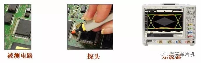


Rolling welded steel pipe: OD 4.76 to 8
Wall thickness:0.5- 0.7
Low carbon steel wire OD 1.0 to 1.8
Bracket:
Steel plate (SPCC) thickness: 0.6 to 1.5
Steel plate (SPCC) thickness: 0.3 to 0.4
2.Structure:
Flat type of Wire On Tube Condenser used at the back
Bended or spiral type of wire on tube condenser used at the bottom
Wrapped type of tube embedded on plate
3.Technical ability:
Wire pitch: ≥ 5mm
4.Performance:
Surface with electrophoresis coating to prevent the corrosion
Inner cleanliness can meet the requirements of CFC and R134a cooling system
Can satisfy the cooling capability requirements