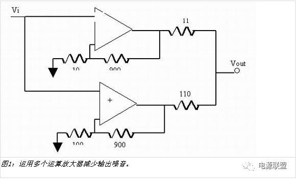
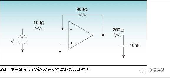
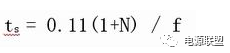
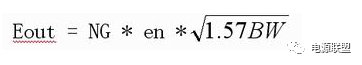
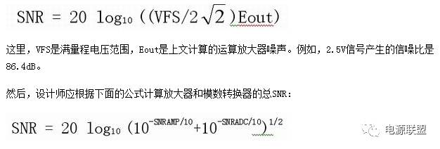
The trend in the modern electronics industry is to integrate more functions into the smallest possible form, which is no secret. Mobile phones are such an example. Many manufacturers today integrate MP3 players, digital cameras and even satellite TV functions into mobile phones. In the past few years, the market has achieved tremendous growth and is still expanding rapidly. The design cycle for these products is usually shorter and the test takes longer than the actual design (the design takes about 4 months and the test takes 6 months). To this end, designers must carefully select devices to avoid repeated modifications and delays in the final product. The following sections highlight some useful design techniques, short calculations, and general assessment methods to help designers better evaluate. In the field of portable electronics, designers use their expertise and best judgment to select devices based on multiple factors (size, cost, and performance). But these factors often require trade-offs, and designers must carefully select components based on the desired end product. Almost as in other industries, the portable market, especially the mobile phone market, typically offers both high-end (multi-function) and low-end (cheap) products. Mobile phone motherboards include different components such as op amps, audio amplifiers and preamps, data converters and ASICs. Before choosing an op amp, designers must consider package options and whether smaller packages will degrade performance. Although small packages are popular in portable products, small packages can cause problems and problems for designers. Operational amplifiers in plastic packages, such as the SC70, often do not achieve the same performance as the corresponding products in SOIC or MSOP packages. The Microchip Chip Scale Package (CSP), which is essentially a die, can be offset by hundreds of orders of magnitude when exposed to light. This package form is also susceptible to cracking during assembly. Which parameters are the most important? In battery-powered applications—especially PDAs and mobile phones—the battery voltage will drop with interference, so choose an op amp with good PSRR performance (~80dB). Also, pay attention to the high gain configuration because the noise coupled into the op amp will cause the noise level to rise. The choice of resistors is also critical, and larger values ​​result in higher noise. Designers can take advantage of 4? Estimate Johnson noise or resistance noise, where R is in K ohms, so a 100K ohm resistor produces about 40nV noise! If multiple op amps are used, one way to reduce noise is to use the scheme shown in Figure 1. This method can reduce the output noise by a factor, where n is the number of amplifiers used. For the LMV651, the output noise will be reduced to approximately 12nV/. In addition, designers must consider limiting bandwidth to minimize noise: designers can use a small capacitor in parallel with a feedback resistor to reduce noise. The choice of op amp also depends on other devices. A common challenge for designers is to choose the right op amp for the analog-to-digital converter (ADC). Although there are many types of data converters on the market, the matching rules between op amps and analog-to-digital converters are different, and designers must carefully consider certain criteria before making a choice. A general review of the data sheets for both devices will provide useful information, but this is not enough. First, select an op amp and an analog-to-digital converter with the same supply voltage. Then select the THD+N small op amp. If you can't find the distortion data, look at the output impedance: an op amp with a small output impedance usually means a smaller THD. Speed ​​is another parameter that must be considered. Although faster op amp speeds are comfortable to use, there are some trade-offs that must be considered, such as higher power and occasional instability. Depending on the ADC selected, the designer should select an amplifier that is at least 50 times faster than the ADC sampling rate. The conversion rate can also be a limiting factor, can the designer base 2? fVp is calculated, where f is the input signal frequency and Vp is the maximum output swing. For example, a 100mV input signal with a frequency of 400kHz (with a gain of 10) requires an amplifier conversion rate of at least 2.5V/μs. Once these basic parameters have been determined, the designer must consider the settling time, which can be misleading. Most manufacturers specify that the op amp's settling time is within 0.1% or 0.01% of a particular input voltage. If the design requires higher accuracy, such as 16 bits, then a parameter in the range of 0.0015% of full scale is required. One way to solve this problem is to estimate the operational amplifier's settling time based on the accuracy of the analog-to-digital converter using the following formula: Here, N is the number of bits and f is the open loop bandwidth of the amplifier. For example, an op amp with a gain of 10, such as the LMV651, has a settling time of approximately 1.4 μs with an accuracy of 12 bits and a 1.65 μs set with an accuracy of 16 bits. This formula is only an approximation. It does not take into account stray capacitance, motherboard inductance, or the input capacitance of the analog-to-digital converter. These factors will affect the settling time. One of the most important indicators before making the final choice is the op amp's noise. A higher noise amplifier reduces the accuracy of the analog-to-digital converter and introduces significant errors into the system. Before starting to calculate the total output noise of the circuit (this can be a very tedious job), it is best to estimate it first. This way the designer knows if the selected amplifier should continue to be used. This estimate relates to the integrated voltage noise of the op amp over the associated bandwidth and the gain of the op amp configuration. We can express this formula as: Here, NG is the noise gain, en is the voltage noise of the operational amplifier, and BW is the closed-loop bandwidth. In the circuit of Figure 2, a simple low pass filter is used at the output. In this example, the output noise is the integrated noise at the filter bandwidth (calculated as 1/2πRC). If a second-order filter is used, the bandwidth is multiplied by a factor of 1.05. Using the above equation and the LMV651 voltage noise density (17nV/), the total output RMS noise of the Figure 2 circuit at 100kHz bandwidth (filter bandwidth) is 53.7V. Once the total output noise is estimated, the designer can calculate the signal-to-noise ratio (SNR) of the op amp using the following formula: The SNR of the ADC121S021 is 72.3dB. When the ADC121S021 is paired with the LMV651, the total SNR is 72.1dB. Ignoring harmonics, the designer can convert this SNR into an equivalent number of bits: ENOB=(SNR-1.76)/6.02, and then only about 0.3dB is lost based on the number of equivalent bits, which is equivalent to 0.03% total accuracy error. . Since noise is integrated noise at a particular bandwidth, it is clear that the noise is also proportional to the bandwidth. In other words, reducing the bandwidth will reduce the noise; expanding the bandwidth will increase the noise. If you decide to choose a higher bandwidth filter, designers should consider choosing a lower noise amplifier. For example, the 10 MHz filter in the circuit of Figure 2 produces a total SNR of less than 71 dB, resulting in a 0.5 bit loss. However, when the LMV791 (5.8nV/) is used with the same filter, the SNR is increased to more than 72dB. Designers can increase the accuracy of the system by simply selecting a lower noise op amp. However, various trade-offs associated with this must be considered, such as power consumption and package size. Other specifications to be considered So far, we have discussed the basic principles and rules for selecting devices for design, but there are other factors to consider. For example, for applications that require higher precision, DC metrics such as input offset voltage and drift can be very important.
The role of Bushing Cover : is the use of non-conductive material will be charged with isolation or wrapped up the characteristics of a safety measure to prevent electric shock. Good insulation to ensure the safe operation of electrical equipment and lines.
Applications:
1. Busbar Insulation Cover can Effectively eliminate short circuit accidents caused by small animals such as birds and animals or foreign body lap.
2. Prevent electrical accidents caused by condensation flash branding, dirty flash branding and icicle sticking to snow.
3. Bushing Covers can prevent acid rain, salt spray and harmful chemical gases from corrosion of transformer inlet and outlet lines.
4. Avoid casualties caused by pedestrians touching exposed electrical contacts by mistake.
5. The protective cover and metering device can be fully closed operation to prevent illegal elements stealing electricity.
6. Buckle structure, simple installation, reusable.
Bushing Cover,Busbar Insulation Cover,Cover Bushing,Bushing Covers CAS Applied Chemistry Materials Co.,Ltd. , https://www.casac1997.com