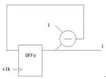
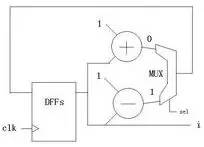
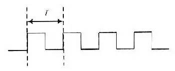
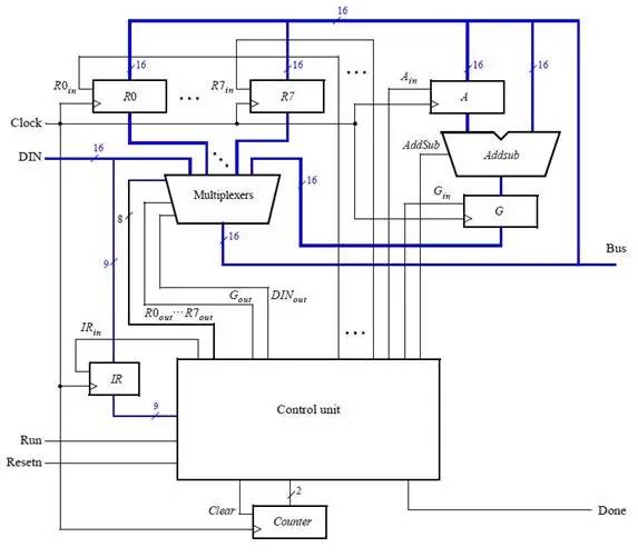
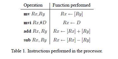
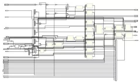
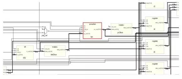
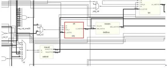
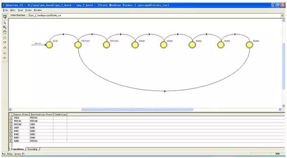
How to make a simple 16-bit CPU, first we have to know what the CPU is doing, presumably everyone is clearer than me. If you want to make a CPU, you must first understand the composition of the computer (or a computer replacement, because not only the computer has a CPU, the current electronic products are very advanced, many devices such as mobile phones, washing machines and even TV and your home The car has to be equipped with a CPU), the digital circuit foundation, it is better to have a little programming basis (of course, no matter it does not matter, this knowledge is easy to obtain, will be mentioned in various books, and in the following process I Will mention this knowledge) What we want to implement is a CPU of a RISC instruction set, and we end up designing instructions and coding for this CPU ourselves. First let's listen to a story about the birth of the CPU: Japanese customers want Intel to help them design and produce eight ASIC chips for desktop calculators. Intel engineers found that there are two big problems with doing this. First, Intel has been working hard to develop three kinds of memory chips, and no manpower to design eight new chips. Second, implementing the calculator with eight chips will greatly exceed the budgeted cost. An engineer from Intel called Ted Hoff carefully analyzed the design of his Japanese counterpart and he discovered a phenomenon. Each of these eight chips implements a specific function. These features are not required at the same time when the user is using the calculator. For example, if the user needs to calculate the sum of 100 numbers, he will repeatedly enter a number, do another addition, do a total of 100 times, and finally print it out. The circuits responsible for input, addition, and printing do not work at the same time. Thus, when a chip is working, other chips may be idle. Hoff has an idea: Why can't you use a common chip plus a program to implement the functions of several chips? When a function is needed, only a piece of program code (called a subroutine) that implements this function needs to be loaded onto the general-purpose chip, and its function is exactly the same as that of the dedicated chip. After a few days of thinking, Hoff drew a new architecture diagram of the calculator, which consisted of four chips: a general-purpose processor chip that implements all computing and control functions; a readable and writable memory (RAM) chip Used to store data; a read-only memory (ROM) chip for storing programs; an input and output chip for inputting data and operating commands, printing results, and so on. After reading this story, you can conclude that the CPU is a device used to replace the ASIC (this is just my understanding, different people have different understandings, this is the wisdom of the wise, I will also be in the next example Explain my thoughts). Then consider the following example: Example 1-1: Mov eax,0 Repeat:inc eax Jmp repeat Example 1-2: Int main() { Unsigned int i = 0; While(1) i++; } Example 1-3: As you can see, the above three examples all produce a sequence that increases from 0, and the first two examples will always be added to the overflow and start from 0 (this depends on the computer's word length and how many bits of CPU, eax is The 32-bit register must be added to 4294967295 and then back to 0, while the latter c program looks different compilers and different platforms. The latter example looks at what adder and how many D flip-flops you use. The question is coming. What if I want to have a descending sequence? The first two examples are very well explained. I can't just change the code directly: Example 2-1: Mov eax,0 Repeat:dec eax Jmp repeat Example 2-2: Int main() { Unsigned int i = 0; While(1) I--; } You just need to tap the keyboard lightly, and after modifying the code, it will execute as you wish. But what about the latter example? Maybe you have already thought of a solution: as shown in Example 2-3. Example 2-3: The problem is coming. You can't change the actual circuit by tapping twice on the keyboard! The above (Example 1-3) is an adder, but when it ran here it became a subtractor (Example 2-3)! In this case, you have to do another circuit, one for arithmetic addition and one for subtraction, but the two circuits represent you have to use more circuits and chips, you have to spend more money, if you can't At the same time, you have spent two money on these two circuits but only done one thing! Can this problem be solved? The answer is yes! Please see example 3: This example uses an adder and a subtractor, no more than the above circuit (obviously... Do you want to use the subtractor as an adder function? Impossible! Of course, plus a negative complement does It is to subtract a number, but here is not considered this problem), a group of multiplexers, a group of D flip-flops. In general, the advantages are obvious (the difference between two boards and one board). The sel signal is used to select (0 is incremented, 1 is decremented). If we regard the sel signal as a "program", this circuit is like a "CPU" that can perform different "operations" according to the "program". In this case, the circuit can be realized by the "program" (sel signal). use. Based on the above conclusions, I think (just personally think ~): The program is an extension of the hardware circuit! The basic idea of ​​the CPU, I think it is like this. Next we analyze the structure of the CPU and the various components, and then implement this CPU. What is a single-cycle CPU, what is a multi-cycle CPU, what is RISC, what is CISC First of all, everyone has to have the concept of a clock: this question is not easy to explain. . . . . . Can be understood as the mechanical clock inside the home, after the battery is ticking away, and its "tick and ticking" speed is the frequency, the time spent ticking is the cycle, and people work, get off work, eat and learn entertainment It is carried out according to the instructions of the clock (the night-end Internet addiction juvenile does not count), in general, the clock signal is generated by the crystal oscillator, 0101 alternating signals (low level and high level). Digital circuits all need a "clock" to drive, just like a conductor is required to play in front of a symphony. All people will follow the commanding tempo, just like all the components in the digital circuit will follow the clock beat. same. The following is an ideal clock signal: (note that it is ideal). Of course, the actual clock signal may not be so ideal, the rising edge may be skewed, and the duty cycle may not be 50%, there is jitter, there is offset (relative to the two devices), probably due to the parasitic capacitance effect of the wire Get out of shape. If you don't understand the above paragraph, it doesn't matter~~~ Anyway, it is telling you that the actual clock signal is definitely not so standard. The working frequency of the CPU is the product of the FSB and the multiplier (how exactly is the cpu frequency, in fact, I am not too clear about this), because the CPU generates a clock signal through an external crystal oscillator, and then passes through the internal circuit ( Phase-locked loop), multiplier to the desired frequency. Of course, some people ask, why is it so troublesome? Just making a clock crystal outside the circuit can produce such a high clock signal. This is ok. On some simple systems (such as 51 single-chip Ji), this is the case, but the calculation of Ji's cpu is more complicated. For some reason, you have to do it inside the cpu. Let's briefly talk about the two instruction sets of the CPU: CISC and RISC. Say my opinion (personal opinion, if there is an error, please ask the expert): RISC is a Reduced Instruction Set Computer, a reduced instruction set computer, a typical example being a MIPS processor. CISC is a Complex Instruction Set Compute, a complex instruction set computer, a typical example is an x86 series processor (of course, the current x86 instruction is still the original cisc instruction, but the actual processor structure has become the risc structure, the structure implementation of risc Pipeline and other features are relatively easy, if you use a series of intel processors in front of the computer, then the instruction set it uses looks like cisc instructions, but in fact your cpu structure is already risc) . Generally, CISC processors need to run with micro-instructions, and RISC is all hard-wired. That is, when cisc's processor executes your program, it must first read some from another rom. The data "guides" how the processor handles your commands, so cisc is less efficient, and risc implements certain functions entirely through the connections between components and components, greatly improving work efficiency, and the emergence of pipeline structures. Provide the foundation. The number of registers in cisc is small, and the instructions can implement some special functions, such as some registers of the 8086: Ax, bx, cx, dx, si, di, etc.; segment registers are: cs, ds, es, ss, etc. The relative instruction function is special. For example, xlat uses the value in bx as the base address, the value in al as the offset, and the data addressed in the memory is sent to al (with ds as the segment register). The risc processor has more general-purpose registers, and the function of the instructions can be slightly weaker, for example: The nios embedded processor shows that the nios processor has 32 general-purpose registers (r0~r31), and the instruction function is weaker than x86, and the x86 memory access is directly using the mov instruction, and the nios processor reads the memory. Is load, write memory is store, The way the two respond to interrupts is different. As a typical example, the x86 processor places the interrupt vector table at the lowest address of the memory (0-1023, each interrupt vector occupies four bytes) and can hold 256. Interrupt (in the real mode of 8086) When responding to an interrupt, load the values ​​of cs and ip at the address corresponding to the interrupt number into the cs and ip registers to save the original address, and save the status register and then enter the interrupt processing. Risco has a common interrupt response function, which finds the address of the function registered by the program to the system based on the interrupt number and calls this function. In general, the length of the cisc instruction used is variable, such as x86 xor ax, bx corresponds to machine code 0x31d8, and push ax is 0x50, pop cx is 0x59. The risc command is indeed fixed length, such as 32 bits. If it is still unclear. . . . . Baidu, it takes a little time to understand these concepts. The basic structure of a CPU and the necessary components This example is referenced from Lab Exercise 9 on the CD from the DE2 Development Board Kit. As you can see from the figure, a CPU contains the general register banks R0~R7, an ALU (arithmetic logic unit), the instruction register IR, and the controller. (Generally this part is a finite state machine or implemented with microinstructions), and there is a data path (connection in the figure). Of course, a real CPU can't contain only a few components. This is a model CPU. That is to say, it just explains the principle of the CPU. A really complicated CPU involves many complicated structures and timings. For example, the virtual mode needs to use some special ones. Registers, page table registers are required to support paging, etc. To speed up memory access, you need to use TLB, speed up access to data and instructions, and use data cache and instruction cache. . . . . Of course, that's all to be considered later, so let's start with this simple part. In the example, the following instructions can be implemented: The mv instruction transfers Ry's data to Rx, mvi transfers the immediate D to Rx, add puts the sum of Rx and Ry into Rx, sub is the same, but performs subtraction. First, let's explain how the mv instruction is executed: the mv instruction shifts the value of Ry into the Rx register. Both registers are composed of a set of D flip-flops, and the number of D flip-flops depends on the width of the register, just like 32-bit machines, 64-bit machines, the number of D flip-flops used by their registers is different. When mv rx, ry is executed, the middle multiplexer (the largest multiplexer in the figure) strobes Ry, and the Ry register drives the bus. At this time, the signal on the Bus is the value of Ry; then it is seen on R0~R7. There are R0in~R7in signals respectively. This signal is the enable signal. When this signal is valid, this trigger will input the data of din on the rising edge. So here we must think of it, this time Din on the Rx trigger. The signal will become active, so that after a clock cycle, the value of Ry is sent to Rx. Similar to the mv instruction, the mvi instruction also sends a data to Rx, except that this time the data exists in the instruction, it is an immediate value, so the Dx signal of Rx will become valid, and the multiplexer will select the data in the IR. Because the immediate number of the mvi instruction exists in the instruction. And perform certain processing, such as extension. The add instruction causes the multiplexer to select Rx first, and then the Ain signal is asserted. After one clock cycle, the Rx data is sent to the A register of Alu. At this time, the multiplexer selects Ry, and the addsub signal is add to indicate the addition of the ALU. Operation, Gin effectively allows the G register to store the operation result, and then the data in the G cycle is the sum of Rx and Ry. At this time, the multiplexer selects Gin, and the Dx of Rx is valid. After one clock cycle, the data is It was stored in Rx. The sub process is similar to add, but the addsub signal is sub indicating that the ALU is subtracting. I made the CPU model Below I will send out the RTL netlist of the CPU model I made, the code I will upload, but this can only be simulated, because the design has problems, there is an asynchronous design, and there is a state machine The output is an error on the clock side of the other device, so this model can only be used for simulation. I used synplify pro to synthesize the RTL, and the state transition diagram was cut off with the Quartus FSM Viewer. The first is an overview of the entire system: This is much more complicated than the simple model above! But don't worry, in fact, this is just the CPU above is a bit more complicated. This is different from the above: this CPU is a multi-cycle CPU and Lab Exercise is a single-cycle CPU. The following figure is the program counter (PC), which is the ip (instruction poiniter) in common x86 processors: The red part is the pc, followed by a three-state bridge, connected to the bus, where the data is sometimes sent to the address bus, used to find the data in the memory, in order to complete the Instruction Fetch process. Sometimes it is sent to the data terminal of the general purpose register to send the value of pc to other registers. The following is IR (Instruction Register), which is a typical feature of multi-cycle processors, because the processor takes the machine code out of memory in the first cycle and then stores it in this register. The latter states are all passed. The data in this register is used as an indication to perform the operation. The following describes the ALU. The ALU is the Arithmetic Logic Unit, the arithmetic logic unit. The function of this device is to perform arithmetic operations and logic operations. Typical arithmetic operation example For example: 1+1=2, 11x23=253, and typical logical operations such as: 1 and 1=1, 0 or 0 = 0, 1<<3=8 This is a logical operation. Let's talk about ADDRMUX: This part is used to select the address, the output on the right is the address bus of the CPU, and the address bus of the CPU has been sent out of the CPU (that is, you can see the pin on the surface of the chip), the address bus of the CPU is It is sent to the address end of the memory, and the modern computer system is actually quite complicated, so in fact, the CPU on your home computer accesses the memory through the North Bridge chip (of course, the memory controller is also implemented in the CPU). The source, the source of the address is a general-purpose register, there is also a program counter, and one is sent directly from the IR, because some of the immediate data also contains memory address information. Finally, the general purpose registers are introduced: Add eax, 2 Equivalent to eax+2 and then sent back to eax. Finally, let's introduce the state machine. This part is the "soul" of the CPU. If there is a "body" in the CPU of the above components, this part is the "soul" of the CPU: The state machine state transition diagram we use is as follows: Because this processor is designed to be very simple, there are not many states. After the processor has gone through the above state, the processor executes an instruction. Some CISC processors are controlled by micro-instructions, and their functions are similar to those of state machines. This structure appears on some older processors. Because the design tools and methods at that time are not as advanced as they are, it is often difficult to change hardware. And high cost, so with the micro-instruction, do a good job of the hardware structure, if you need to change as long as you modify the micro-instruction, and now the electronic technology is very developed, the design tools are also very complete, so there are many directly through the hard A processor that is wired. Good horse with a good saddle, with a processor, we have to give it a good program, below we use the processor we designed to sum, from 1 to 100, because we did not design the compiler, also The assembler is not designed, so the program can only be written in machine code. The sample program is as follows: We may wish to write the assembly code of the program first: Mov [ADDR],r0;r0 = 0 Mov r1,100 Lop:add r2,r1 Sub r1,1 Cmp r1,0 Jz ext Mov r4,4 Jmp r4(lop) Ext:mov [ADDR],r2 Jmp $ The address of the data stored in the memory is first cleared, so that the result of the subsequent transmission can be stored, and then the r1 register is stored in the number of loops (that is, the upper limit of the summation). Then add the value of r1 to r2, r2 is actually the register of the summation, and finally we will send the value in r2 to an address in memory. Then subtract 1 from r1 to see if it is 0? If it is 0, it means the sum is over. If it is not 0, it means to continue. After the end, the program jumps to the ext part and stores the result in an address in the memory (in the example, 49152 is the binary 1100000000000000b). Finally jmp $ is to stop the program in this line, to prevent the program from running away (the program that runs away is very harmful! It is possible to use the data as code or the code as data!) Convert to VerilogHDL language as follows: Module memory ( Input [15:0] addr, Inout [15:0] data, Input rw ); Reg [15:0] data_ram[0:16'b1111_1111_1111_1111]; Integer i; Initial begin For (i = 0; i <= 16'b1111_1111_1111_1111; i = i + 1) Data_ram[i] = $random(); Data_ram[0] = 16'b1000000100000000; //mov [ADDR],r0;r0 = 0 Data_ram[1] = 16'b1100000000000000; //ADDR Data_ram[2] = 16'b1000000010001000; //mov r1,100 Data_ram[3] = 100; //100 //data_ram[2] = 16'b1110011001000000; Data_ram[4] = 16'b0010000100010001; //lop:add r2,r1 Data_ram[5] = 16'b1110000011001000; //sub r1,1 Data_ram[6] = 16'b0000000000000001; //1 Data_ram[7] = 16'b1110000000001000; //cmp r1,0 Data_ram[8] = 16'b0000000000000000; //0 Data_ram[9] = 16'b1110011010000000; //jz ext Data_ram[10] = 16'b0000000000000011; //+3 offset(ext) Data_ram[11] = 16'b1000000010100000;//mov r4,4 Data_ram[12] = 16'b0000000000000100; Data_ram[13] = 16'b0110011001100000;//jmp r4(lop) Data_ram[14] = 16'b1000000100000010;//ext:mov [ADDR],r2 Data_ram[15] = 16'b1100000000000000;//ADDR Data_ram[16] = 16'b1110011001000000;//jmp $ Data_ram[17] = 16'b1111111111111110;//-2 offset($) /*data_ram[0] = 16'b1000000010000000; //mov r0,imm Data_ram[1] = 16'b0011111111111111; //imm Data_ram[2] = 16'b0000000001111000; //mov r7,r0 Data_ram[3] = 16'b1000000010011000; //mov r3,0 Data_ram[4] = 16'b0000000000000000; Data_ram[5] = 16'b1000000010100000; //mov r4,code of jmp r5 Data_ram[6] = 16'b0110011001101000; //jmp r5 Data_ram[7] = 16'b0000000101011100; //mov [r3],r4 Data_ram[8] = 16'b1000000011110000; //mov r6,[0] Data_ram[9] = 16'b0000000000000000; //[0] Data_ram[10]= 16'b1000000100000110; //mov [255],r6 Data_ram[11]= 16'b0000000011111111; Data_ram[12]= 16'b0110011001011000; //jmp r3 */ End Always @ (addr or rw or data) If (rw) Data_ram[addr] = data; Assign data = rw ? 16'hzzzz : data_ram[addr]; Endmodule In the design, the CPU peripheral also needs a memory device (Memory). I model it with HDL. When initializing, the corresponding data at each memory address is initialized to random, and then only a series of addresses starting from 0 are initialized to The code I wrote, the assembly instructions for the machine code are given in the comments. Then the result, the result should be that r2 changes from 0 to 5050 (1+2+3+...+100=5050) And r1 changes from 100 to 0. After changing to 0, the program will enter an infinite loop and stop at jmp$. This is when the simulation starts: And as you can see, d2 changes from 0 to 0x64, which is the decimal 100, indicating that the first addition has been performed. Let's see the end of the simulation: Finally, I will give some instructions that I use (similar to x86): Add dst, src adds src and dst and sends them to the dst register Mov [addr], src sends the value of src to the memory location with the address of addr Sub dst, src subtracts dst from src and sends it to dst Cmp dst, src minus dst minus src and then not sent to dst to change only the flag bit Jz dst jumps to dst when zf=1 (that is, the result of the last arithmetic operation is 0) Finally, let me mention: I used synplify integrated circuit, and then simulated with debussy+modelsim, 3.2V Battery Cells,Prismatic Phosphate Lithium Batteries,3.2V 202Ah,3.2v lifepo4 battery,3.2V LifePO4 Lithium Battery Pack Jiangsu Zhitai New Energy Technology Co.,Ltd , https://www.zt-tek.com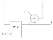
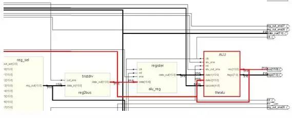
As you can see from the figure, the output of the ALU is connected to the back with a long line. If you refer to the diagram of the entire CPU, you will find that these lines are connected to the general-purpose registers. This is to save the results of the operation. For example, if you use add eax, 1, the value of eax is incremented by 1 and then returned to eax, so the result of the ALU is sent back to the general-purpose register with feedback, and the input of the ALU should also have the output of the general-purpose register. 
The purpose of a general purpose register is to hold intermediate values ​​or for operations, such as 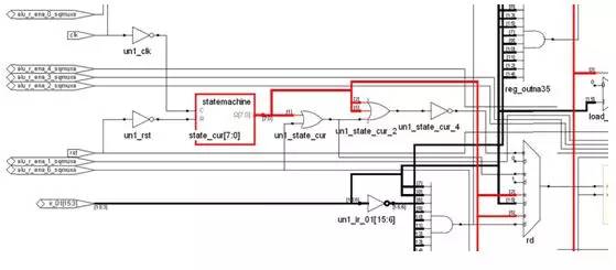
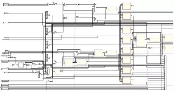
The state machine is basically connected to all the components of the system, because the execution of all the actions mentioned above requires the control of the state machine. The state machine is actually composed of a memory circuit composed of a part of the flip-flops and another combination of logic. The configuration of the secondary decoding circuit, as well as the decoding according to the current state and input, is used to control the various components. The following is a typical FSM structure in the textbook: 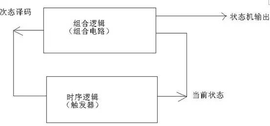
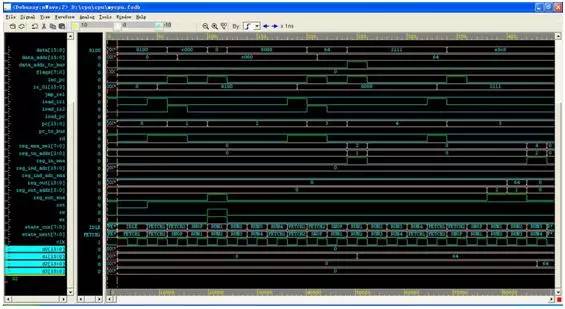
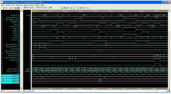
At this time, d1 changes to 0 and d2 changes to 0x13ba (5050 in decimal), indicating that the program has been run in the processor we designed and the result is successful!