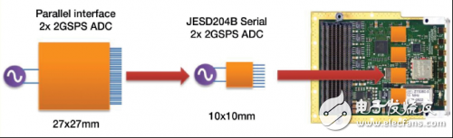
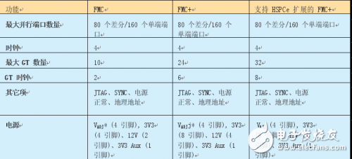
The updated FPGA mezzanine card specification provides unparalleled high I/O density and backwards compatibility. As an important development in embedded computing design using FPGAs and high-speed I/O, the latest mezzanine card standard called FMC+ will extend the total number of Gigabit Transceivers (GTs) in the card from 10 to 32, the largest The data rate has been increased from 10Gbps to 28Gbps while maintaining backward compatibility with current FMC standards. These features also fit well with new devices using the JESD204B serial interface standard, as well as 10G and 40G optics and high-speed serial memories. FMC+ meets the most challenging I/O requirements, giving developers a double benefit: the flexibility of mezzanine cards and the high I/O density of single-chip designs. The FMC+ specification was developed and refined last year. The VITA 57.4 working group has approved the specification and will submit an ANSI vote in early 2016. Let's take a closer look at this important new standard and understand its impact on advanced embedded design. Advantages of mezzanine cards Mezzanine cards are an effective and widely used method of adding specific functionality to embedded systems. Because the mezzanine card is attached to the base card or carrier card rather than directly to the backplane, the mezzanine card can be easily replaced. For system designers, this means both flexible configuration and easy upgrades. However, due to connectivity issues or the extra space required to install on the development board, this flexibility often comes at the expense of functionality. For FPGAs, the main open standard is ANSI/VITA 57.1, also known as the FPGA Mezzanine Card (FMC) specification. The latest standard, FMC+ (more formally, VITA 57.4) extends the capabilities of the existing FMC standard by significantly enhancing the functionality of the Gigabit serial interface. Compared to single-chip solutions, FMC+ addresses many of the deficiencies of mezzanine-based I/O while providing greater flexibility and performance. At the same time, the FMC+ standard is backward compatible, in line with the development history of FMC and meet the needs of its user community. The FMC standard defines a small mezzanine card that is similar in height and width to a mature MMC or PMC, but only half the length. This means that FMC has a smaller board-level space than the open standard format. However, FMC does not require a bus interface that often takes up a lot of board space, such as PCI-X. Instead, the FMC communicates with the master FPGA using a direct-connect I/O with a relatively simple power supply requirement. This means that although the size is smaller, the FMC actually Like the XMC equivalent of their larger I/O capacity and the PMC and XMC specifications, both FMC and FMC+ offer both air cooling and conduction cooling, so both commercial and military markets demand common and durable applications. Can be applied. The FMC specification is fairly straightforward to parse. The standard provides up to 160 single-ended or 80 differential parallel I/O signals for high pin count (HPC) designs, providing half the number of I/O signals for low pin count (LPC) designs. Up to 10 full-duplex GT connections can be set. These GTs are suitable for fiber optics or other serial interfaces. In addition, the FMC specification defines key clock signals. All of these I/Os are optional, although most hosts now support full connectivity. The FMC specification also defines a variety of power inputs, although the mezzanine card defines the power supply from the host. This method works by first powering the mezzanine card section so that the host can interrogate the FMC and then the FMC responds by defining a voltage range for the VADJ. If the host is able to provide this voltage range, everything goes smoothly. Not setting the main power adjustment on the mezzanine card can save space and reduce the power consumption of the mezzanine card. FMC for analog I/O Designers can use FMC as a feature that any user wants to connect to an FPGA, such as digital I/O, fiber optics, control interfaces, memory, or additional processing. However, analog I/O is still the most common use of FMC technology. The FMC specification applies to a wide range of fast, high-precision I/O, but it also needs to be weighed, especially for high-speed components that use parallel interfaces. For example, Texas Instruments' ADC12D2000RF dual 2 Gsps 12-bit ADC uses a 1:4 multiplexed bus interface, so this bus speed is not too fast for the master FPGA. The digital data interface requires 96 signals alone (48 LVDS pairs). For this class of devices, the FMC can only support one such device, and the FMC has an upper limit of 160 signals, even if there is enough room for more devices. Even lower precision devices operate at higher speeds, such as those operating on 8-bit data channels, allowing for more channel counts even with higher front-end analog coupling requirements for converters, amplifiers, clocks, and more. For analog interfaces that use a parallel interface running at 5 Gsps or 6 Gsps (throughput greater than 50 Gbps) with accuracy greater than 8 bits, the FMC specification cannot begin to cope. From a market perspective, mainstream FMC throughput is between 25-50 Gbps in terms of channel density, speed and accuracy. This level of performance is the result of the physical package size and the available connections to the master FPGA. In addition to parallel connections, the FMC specification supports up to 10 duplex high speed serial (GT) links. Figure 1 - FMC reduces the impact of packaging with JESD204B Table 1 - FMC and FMC+ Connections These interfaces are useful for emerging technologies such as fiber I/O, Ethernet, Hybrid Memory Cube (HMC) and Bandwidth Engine, and next-generation analog I/O devices that use the JESD204B interface. JESD204B coming Although the JESD204 serial interface standard (currently revision "B") has been around for a while, it has only recently been widely adopted by the market as a serial interface standard for a new generation of high sample rate data converters. The driving force behind this widespread adoption comes from the telecommunications industry's desire for smaller, lower power and lower cost devices. As mentioned earlier, dual-channel 2 Gsps, 12-bit ADCs with parallel interfaces require a large number of I/O signals. This requirement directly affects the package size. In this case, a 292-pin package is required, which is approximately 27x27mm (although the next-generation pin geometry can shrink package size to less than 20x20mm). The equivalent device with JESD204B connection can be packaged in a 68-pin, 10x10mm package with lower power consumption. This shrinking package size is well matched to evolving FPGAs as FPGAs are providing an ever-increasing number of GT links that are growing in speed. Figure 1 shows an example of the package size and the FMC/FMC+ development board size. Depending on the data throughput, accuracy, and number of analog I/O channels required for the sample rate, a typical high speed ADC and DAC using the JESD204B interface has 1-8 GT links operating at 3-12 Gbps. The FMC specification defines a relatively small-sized mezzanine card, but with the rise of the JESD204B device, more components can be accommodated in the board-level space. Up to 10 GT links defined by the FMC specification are one available. It is this limited number of GT links that can provide 80 Gbps or higher throughput by using only a fraction of the number of pins required for parallel I/O. The rise of serial-connected I/O devices using interfaces such as JESD204B has indeed brought deficiencies to some of the subdivision applications of electronic warfare, such as digital radio frequency memory (DRFM). Due to the long data pipeline, serial interfaces inevitably bring greater Delay. For DRFM applications, the delay between data input and data output is a fundamental performance parameter. While the delays between serial connected devices tend to be very different, next-generation devices will allow data to pass through the pipeline at a faster and faster rate, some of which are expected to have the ability to adjust the pipeline depth. It remains to be seen how much improvement can be achieved. Antenna For Automotive Product,Fm Transmitter Antenna,Radio Transmitter Antenna,Transmitting And Receiving Antenna IHUA INDUSTRIES CO.,LTD. , https://www.ihuagroup.com